Paper Sharing
【Domestic Papers】High-Performance ε-Ga₂O₃ Photodetectors Based on Two-Step Growth to Expand Carrier Transport Paths for Solar-Blind Imaging Applications
日期:2026-05-15阅读:28
Researchers from Shandong University and University of Science and Technology of China have published a dissertation titled “High-Performance ε-Ga₂O₃ Photodetectors Based on Two-Step Growth to Expand Carrier Transport Paths for Solar-Blind Imaging Applications” in Advanced Optical Materials.
Background
Solar-blind ultraviolet photodetectors are crucial for fire monitoring, military early warning, corona detection, and other fields. ε-Ga₂O₃ is an ideal candidate due to its ultra-wide bandgap, high absorption coefficient, and excellent stability. Traditional heteroepitaxy easily leads to rotational domains and lattice defects, resulting in poor film quality and high dark current. Intrinsic ε-Ga₂O₃ has low carrier concentration, limiting the separation and transport of photogenerated carriers. Meanwhile, a single transport path cannot achieve both high photoresponse and fast response simultaneously. At present, studies on combining two-step growth and Ge doping to construct dual carrier transport paths, improve film crystallinity, and realize high-performance solar-blind imaging arrays are still insufficient.
Abstract
ε-Ga₂O₃ is considered a promising candidate for fabricating high-performance solar-blind photodetectors (SBPDs) due to its excellent thermal stability, compatibility with heterogeneous integration, and the capacity for achieving high gain through defect engineering. In the future, there is an urgent need to design and fabricate Ga₂O₃-based photodetectors with high sensitivity for practical applications. Herein, we firstly present a two-step growth to enhance the performance of ε-Ga₂O₃-based SBPDs. The fabricated SBPDs based on these films achieve a high specific detectivity of 2.79 ×10¹⁶ Jones, a responsivity of 407.5 A W⁻¹ and a fast response speed with a decay time of 48 ms, representing one of the highest detectivity values reported for ε-Ga₂O₃-based SBPDs. Due to the introduction of the low-temperature buffer layer, the quality of the epilayer has been improved, the leakage channel of the epilayer is compensated, and the dark current is reduced. Additionally, a device with a bilayer structure has two paths for carrier transport under illumination, which greatly increases the photocurrent. Furthermore, as a proof-of-concept application, a 5 × 5 photodetector array using Ge-doped ε-Ga₂O₃ epitaxial wafers successfully captured clear images. This work provides a feasible strategy for developing ε-Ga₂O₃ SBPDs with high sensitivity and rapid response characteristics.
Highlights
A two-step growth method is proposed to improve the crystallinity of ε-Ga₂O₃ films and reduce dark current.
Dual carrier transport paths are constructed in bilayer structure to significantly enhance photocurrent and responsivity.
The Ge-doped ε-Ga₂O₃ photodetector achieves a record high detectivity of 2.79 ×10¹⁶ Jones.
A 5 × 5 high-uniformity photodetector array is fabricated for clear solar-blind imaging.
Low-temperature buffer layer effectively alleviates lattice mismatch and defect propagation.
Conclusion
High-performance Ge-doped ε-Ga₂O₃ SBPDs are fabricated using the two-step growth. The two-step growth has been proven to alleviate lattice mismatch, thus ensuring excellent morphology and crystal quality of ε-Ga₂O₃ films. In addition, the two carrier transport paths are also the reasons for the performance improvement of these photodetectors. The Ge-doped ε-Ga₂O₃ SBPDs exhibited excellent optical response performance: PDCR = 6.11 ×10⁷, R = 407.5 A/W specific D* = 2.79 ×10¹⁶ Jones, and response time = 0.5805 / 0.0484 s. Based on the superior performance of the ε-Ga₂O₃ SBPDs, a 5 × 5 SBPD array for high-resolution solar-blind imaging was fabricated, demonstrating that ε-Ga₂O₃ SBPDs have significant potential for practical applications in solar-blind detection and DUV imaging. This work advances the development of high-performance ε-Ga₂O₃ SBPDs for large-scale, high-resolution array imaging applications.
Project Support
We gratefully acknowledge financial support from the Natural Science Foundation of Shandong Province (ZR2023ZD05), the Shenzhen Fundamental Research Program (Grant Number. GJHZ20220913142605011), the National Key Research and Development Program of China (2024YFA1208800), the National Natural Science Foundation of China (Grant Number.52572177), the Taishan Scholar Foundation of Shandong Province under Grant tsqn202408337.
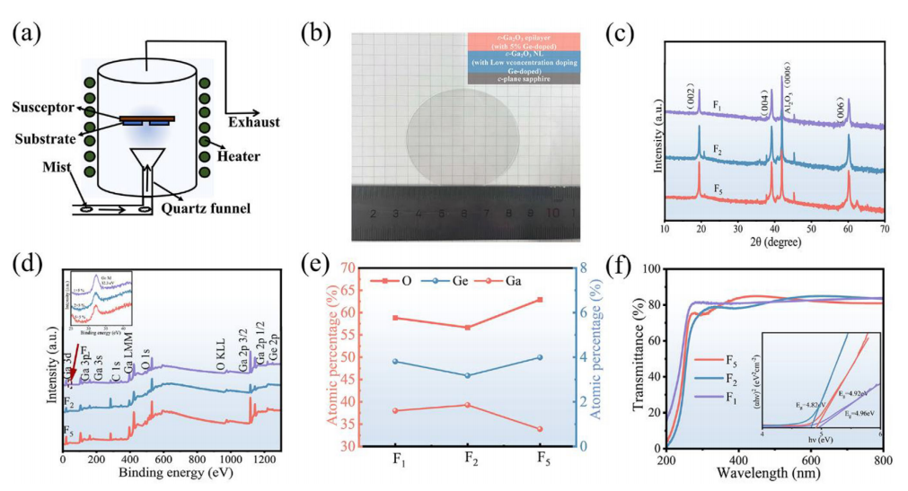
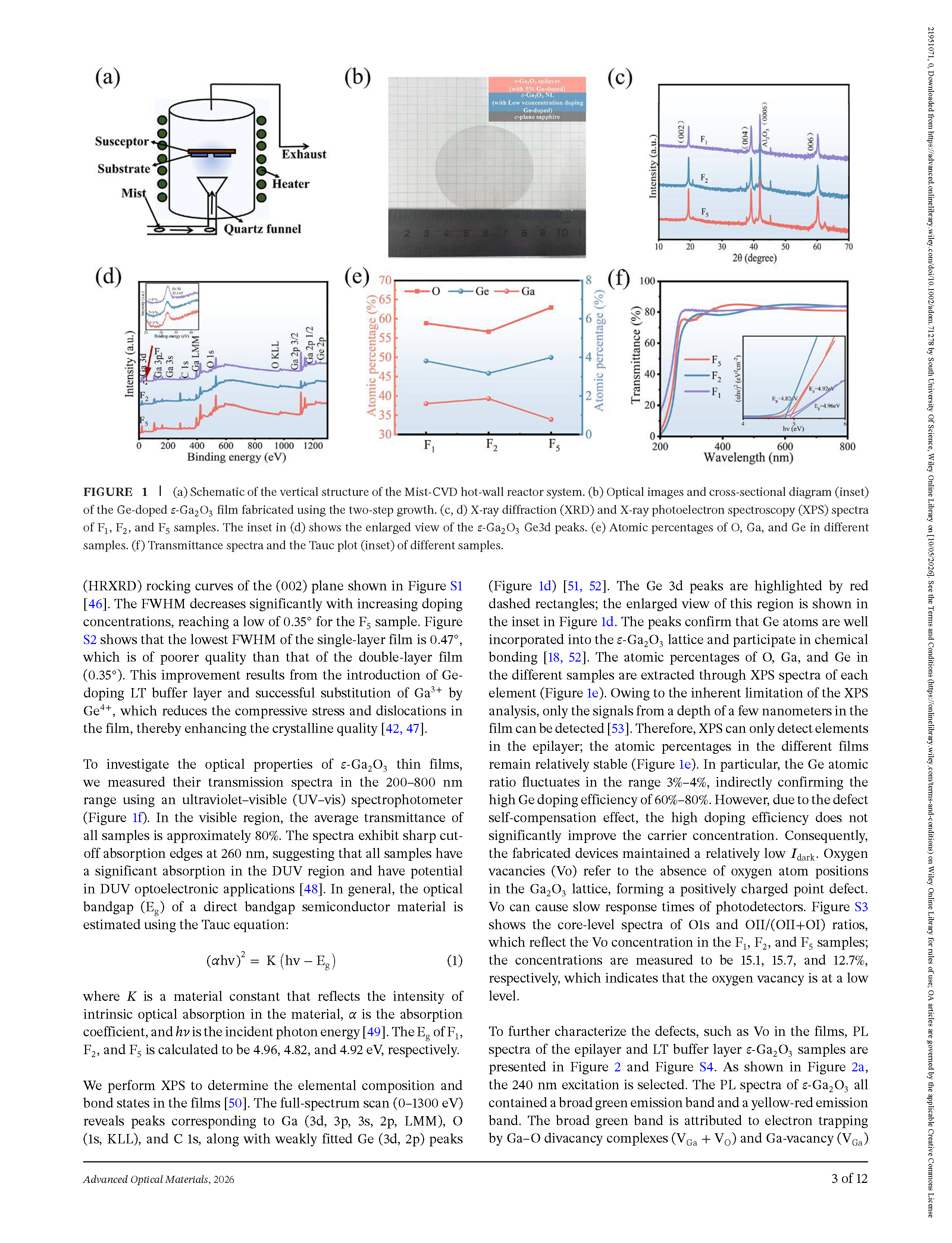
FIGURE 1. (a) Schematic of the vertical structure of the Mist-CVD hot-wall reactor system. (b) Optical images and cross-sectional diagram (inset) of the Ge-doped ε-Ga₂O₃ film fabricated using the two-step growth. (c, d) X-ray diffraction (XRD) and X-ray photoelectron spectroscopy (XPS) spectra of F₁, F₂ and F₅ samples. The inset in (d) shows the enlarged view of the ε-Ga₂O₃ Ge 3d peaks. (e) Atomic percentages of O, Ga, and Ge in different samples. (f) Transmittance spectra and the Tauc plot (inset) of different samples.
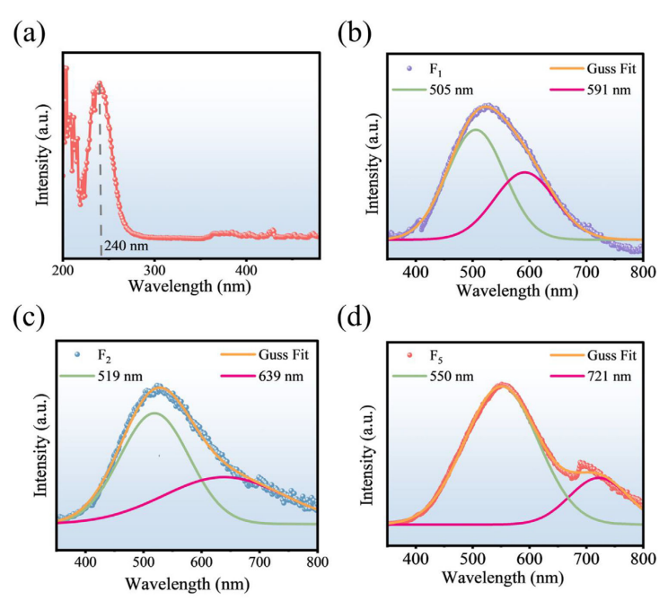
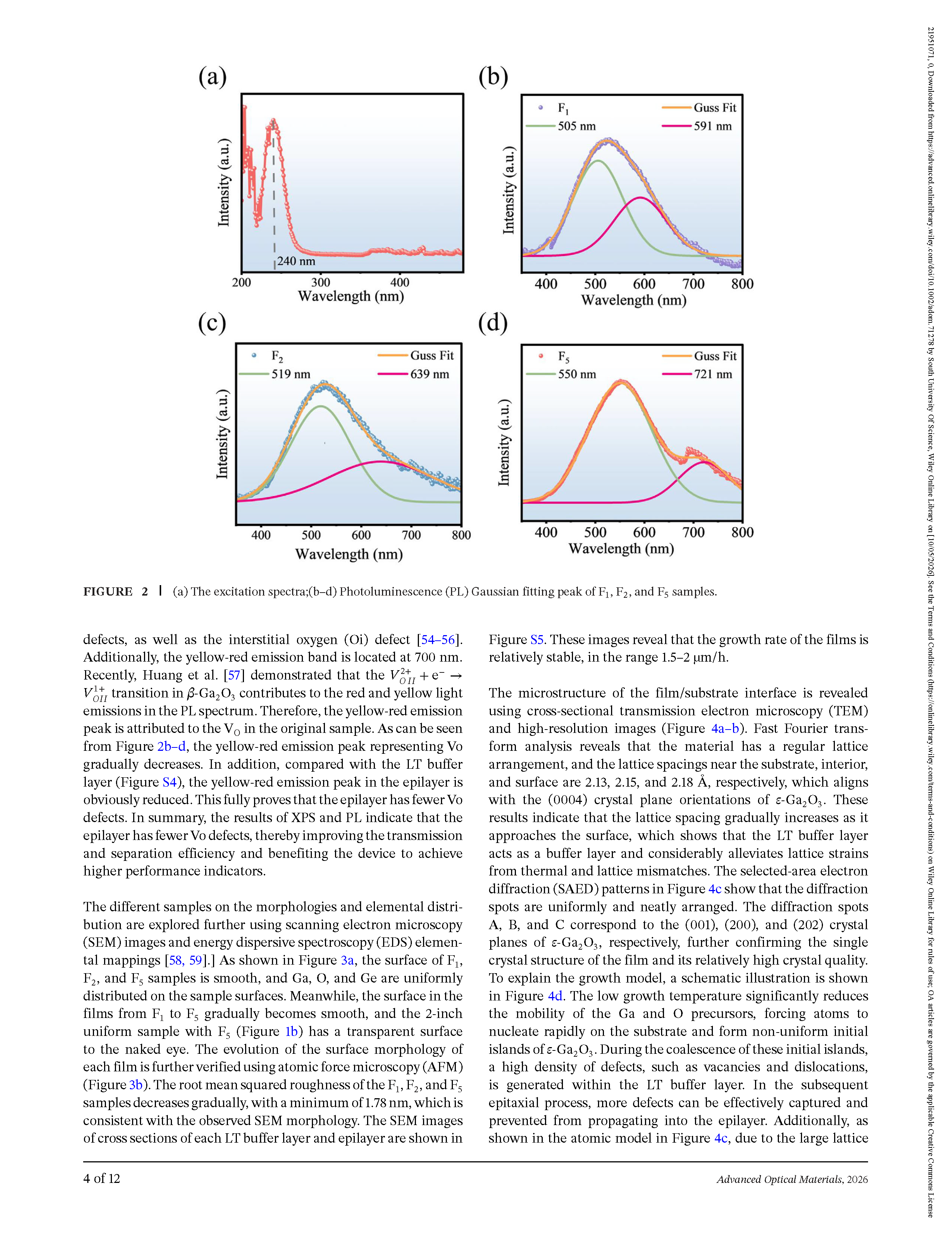
FIGURE 2. (a) The excitation spectra; (b–d) Photoluminescence (PL) Gaussian fitting peak of F₁, F₂, and F₅ samples.
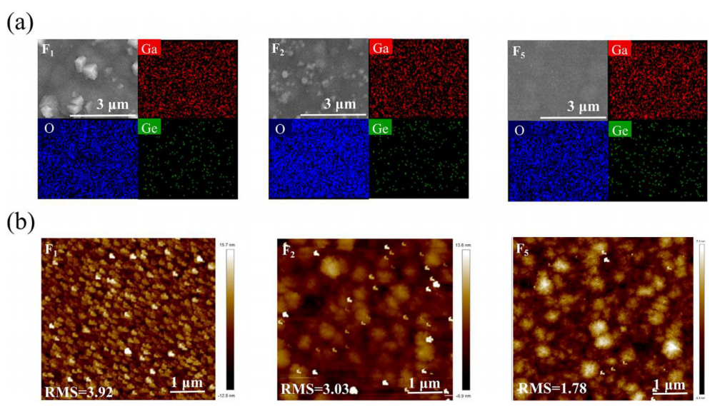
FIGURE 3. (a) Scanning electron microscopy (SEM) images and energy dispersive spectroscopy (EDS) elemental mappings, and (b) Atomic force microscopy (AFM) morphologies of F₁, F₂, and F₅ samples in epilayers.
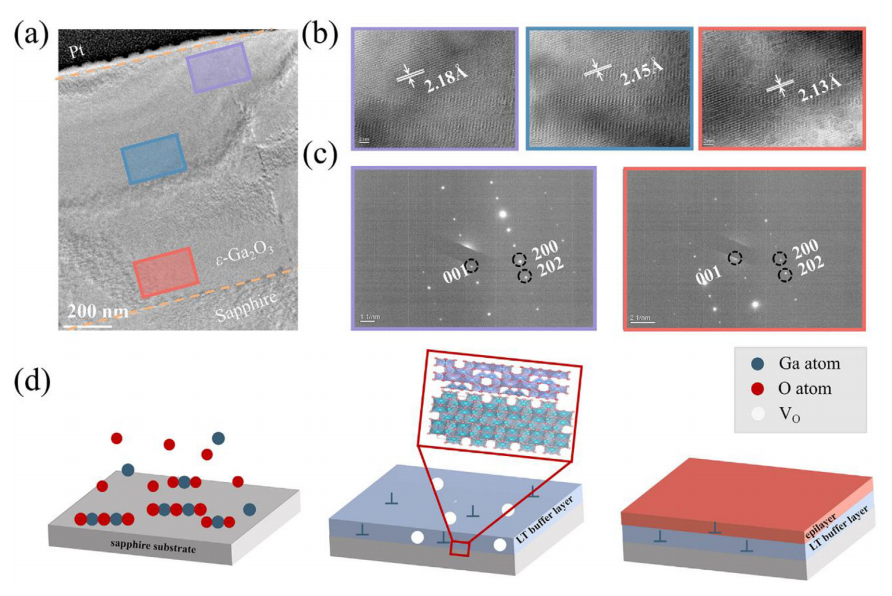
FIGURE 4. (a, b) Transmission electron microscopy (TEM) and high-resolution images of selected areas in F₅. (c) Selected-area electron diffraction (SAED) patterns from the selected region shown in (b). (d) Schematic diagrams of ε-Ga₂O₃ structure revolution.
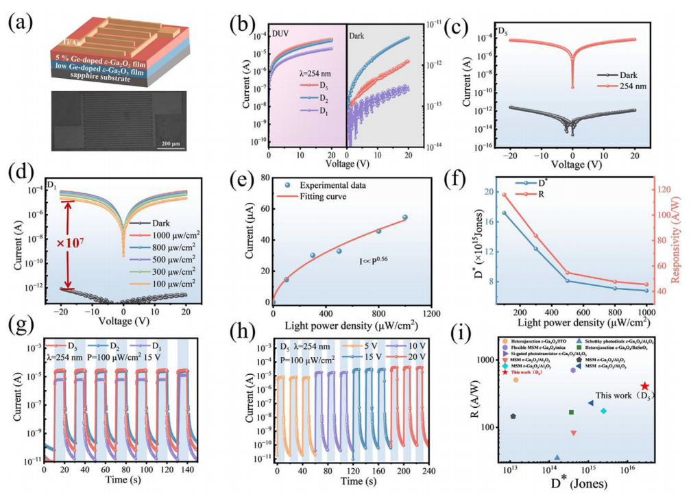
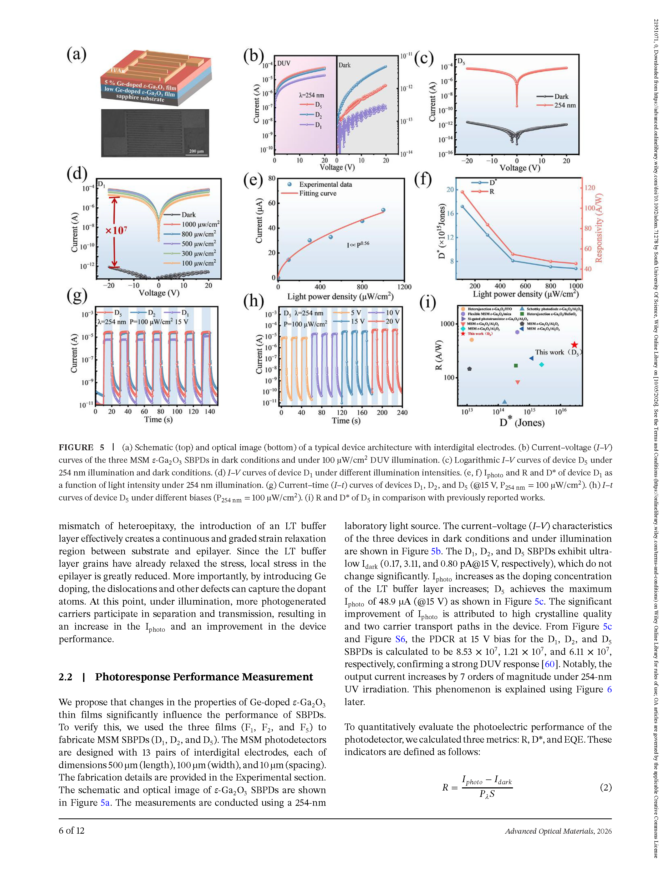
FIGURE 5. (a) Schematic (top) and optical image (bottom) of a typical device architecture with interdigital electrodes. (b) Current–voltage (I–V) curves of the three MSM ε-Ga₂O₃ SBPDs in dark conditions and under 100 μW/cm² DUV illumination. (c) Logarithmic I–V curves of device D₅ under 254 nm illumination and dark conditions. (d) I–V curves of device D₁ under different illumination intensities. (e, f) Iphoto and R and D* of device D₁ as a function of light intensity under 254 nm illumination. (g) Current–time (I–t) curves of devices D₁, D₂, and D₅ (@15 V, P₂₅₄ nm = 100 μW/cm²). (h) I–t curves of device D₅ under different biases (P₂₅₄ nm = 100 μW/cm²). (i) R and D* of D₅ in comparison with previously reported works.
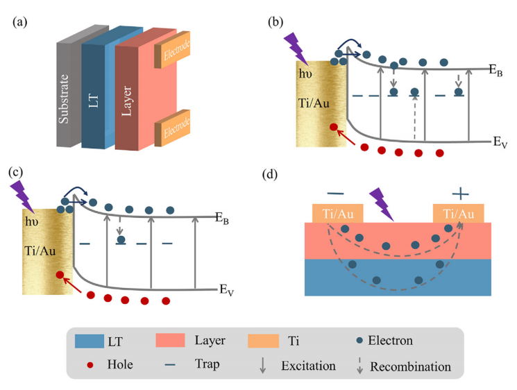
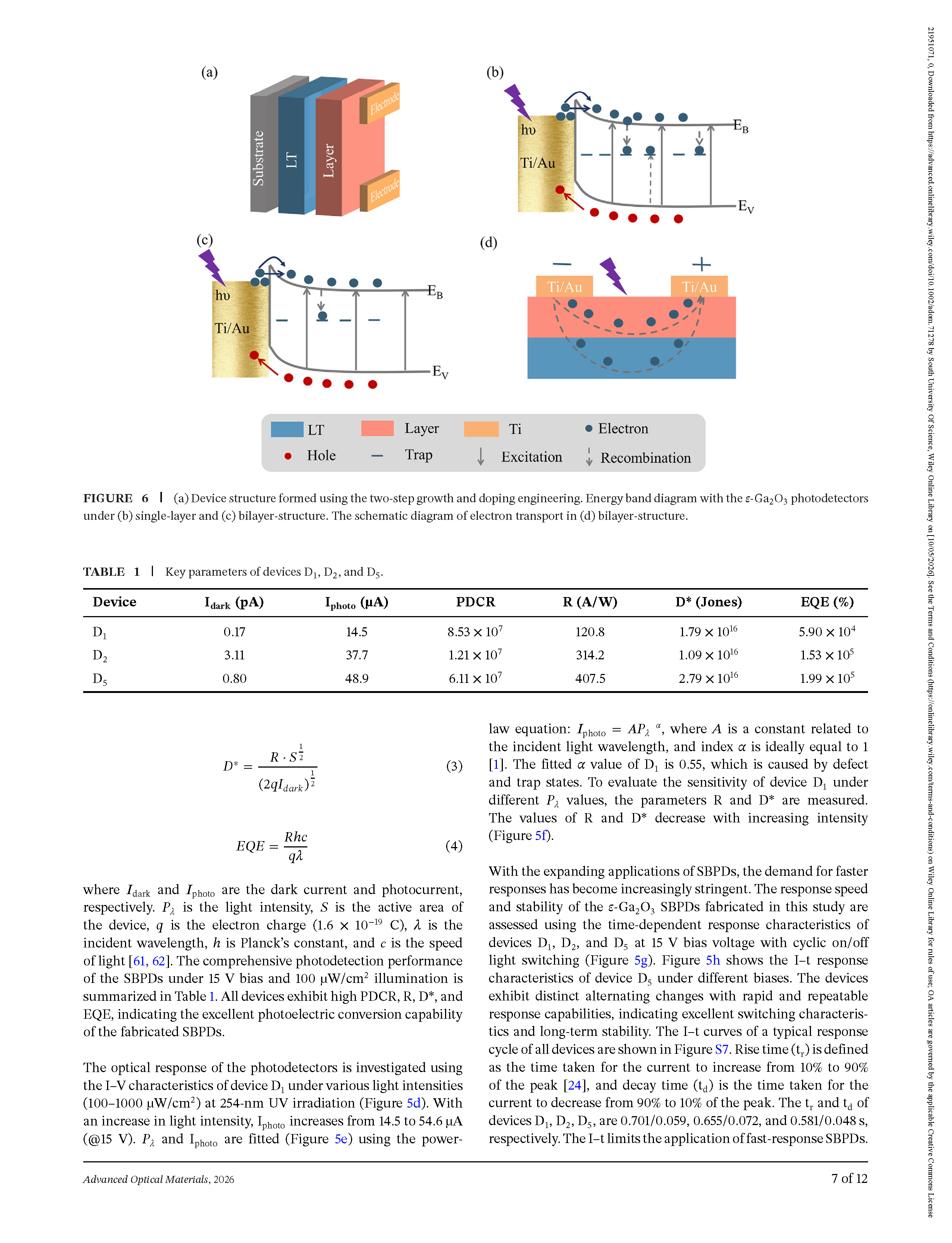
FIGURE 6. (a) Device structure formed using the two-step growth and doping engineering. Energy band diagram with the ε-Ga₂O₃ photodetectors under (b) single-layer and (c) bilayer-structure. The schematic diagram of electron transport in (d) bilayer-structure.
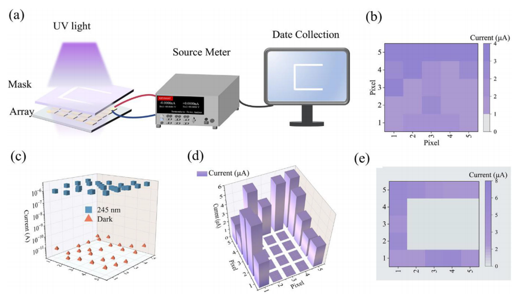
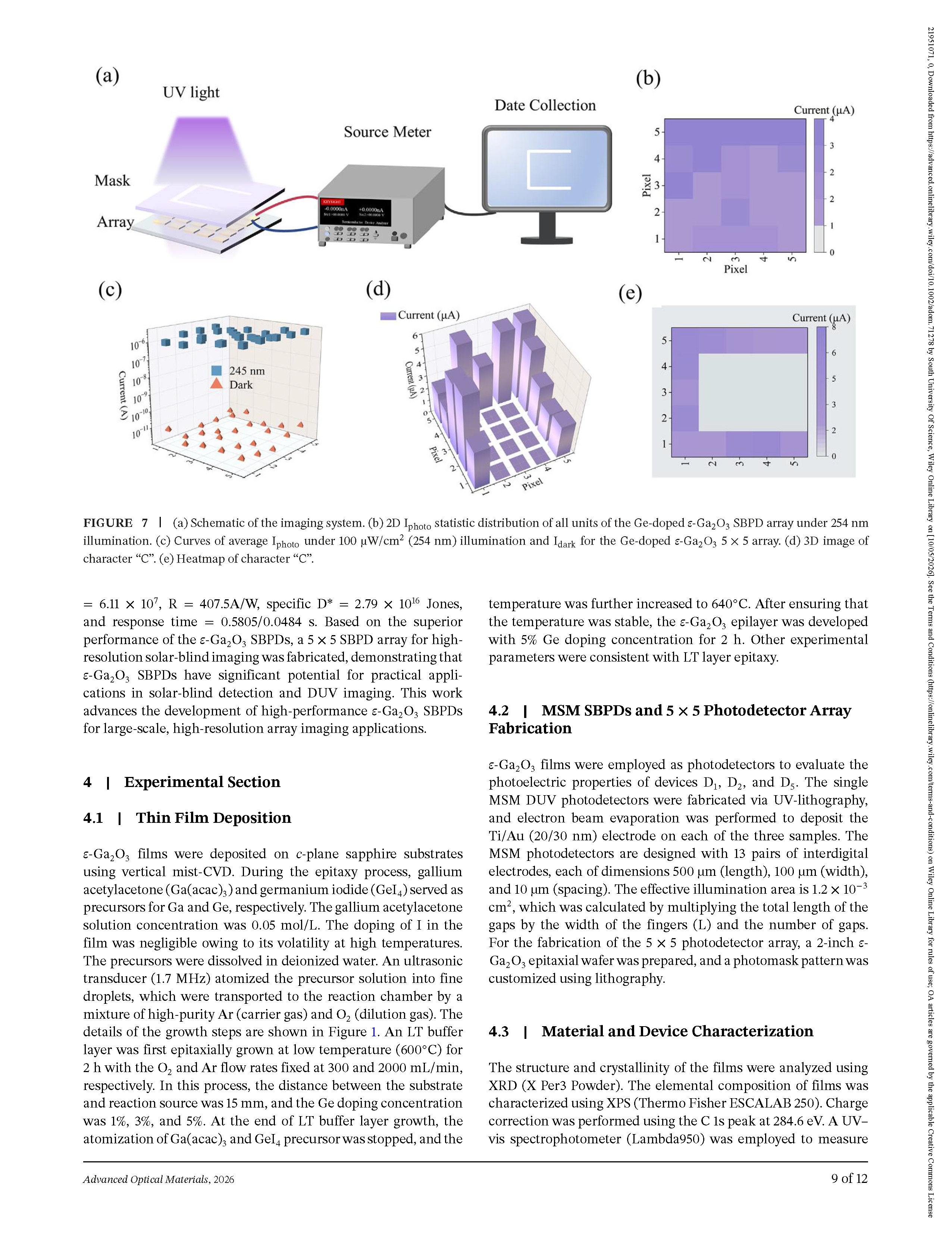
FIGURE 7. (a) Schematic of the imaging system. (b) 2D Iphoto statistic distribution of all units of the Ge-doped ε-Ga₂O₃ SBPD array under 254 nm illumination. (c) Curves of average Iphoto under 100 μW/cm² (254 nm) illumination and Idark for the Ge-doped ε-Ga₂O₃ 5 × 5 array. (d) 3D image of character “C”. (e) Heatmap of character “C”.
DOI:
doi.org/10.1002/adom.71278