Paper Sharing
【International Papers】Electrostatic effects of self-trapped holes in β-Ga2O3 devices
日期:2026-05-11阅读:34
Researchers from the Ohio State University have published a dissertation titled " Electrostatic effects of self-trapped holes in β-Ga2O3 devices" in Applied Physics Letters.
Background
β-Ga2O3 is a promising new semiconductor material. It has several attractive attributes-a Baliga Figure of Merit that is higher than that of its competitors SiC and GaN, several shallow n-type dopants with usable solubilities, an ultra-wide bandgap of 4.5-4.8 eV, and a critical breakdown field of 6-8 MV/cm. Despite its many strengths, β-Ga2O3 is not without limitations. Two principal challenges hinder its development: intrinsically low thermal conductivity and lack of p-type material. The lack of shallow acceptor dopants precludes the formation of conventional p-n junctions, thereby requiring device designers to use unique architectures to perform those functions.
Abstract
β-Ga2O3 is an ultra-wide bandgap semiconductor with exceptional properties for power electronics and UV-C optoelectronics, but its behavior under illumination remains poorly understood. In this work, we investigate how optically generated self-trapped holes influence electrostatics and current conduction in β-Ga2O3 devices. Using a vertical Schottky photodiode with a semi-transparent Ni anode, we performed capacitance–voltage (C–V), current–voltage (I–V), and temperature-dependent I–V measurements under dark and above-bandgap illumination. Analysis of photocurrent gain reveals that conventional image-force barrier-lowering models require unrealistically high interfacial electric fields, suggesting the presence of an alternative mechanism. By applying the Fowler–Nordheim tunneling theory, we reconcile measured photocurrents and photo-capacitance results with physically plausible fields and quantify the two-dimensional concentration of self-trapped holes. Our findings demonstrate that illumination-induced charge significantly alters device electrostatics. Understanding this tunneling-based photocurrent gain mechanism is critical for designing β-Ga2O3 devices for UV-C detectors and power electronics.
Highlights
The traditional image-force barrier-lowering model is overturned, and the photoconductive gain of β-Ga2O3 Schottky detectors is confirmed to originate from Fowler-Nordheim tunneling.
The areal density and centroid position of illumination-induced self-trapped holes are quantitatively extracted, revealing their mechanism of reshaping internal electric field and energy band.
Temperature-dependent electrical measurements exclude contributions from interface states and thermionic emission, providing direct experimental evidence for electrostatic modulation by self-trapped holes.
Conclusion
In summary, we have shown how charge, field, and energy band profiles of β-Ga2O3 photodetectors change upon illumination with above-bandgap light because of excess charges introduced by optically generated self-trapped holes based on the evidence provided by I–V, C–V, and I–V–T measurements in dark and illuminated conditions. β-Ga2O3 provides a rather unique case of a semiconductor with excellent transport properties which also has self-trapped holes. While the presence of self-trapped holes in illuminated β-Ga2O3 devices is well established, this work shows the impact of polarons on device electrostatics and current characteristics. Our results show that the photoconductive gain in β-Ga2O3 Schottky photodetectors originates from electron tunneling from the metal into the semiconductor, rather than from thermionic emission enhanced by image-force barrier lowering. We show that hole-induced tunneling uniquely explains the current–voltage behavior typically reported in Ga2O3 optoelectronic devices, and we provide a quantitative, experimentally validated, physics-based rationale for this mechanism. By adopting a model that includes tunneling of electrons from the metal, we reconcile measured photocurrents with physically plausible electric fields, extract a two-dimensional concentration of self-trapped holes which reshape the internal field profile, and estimate the energy band diagram at a range of voltages. Understanding this tunneling-based gain mechanism and, more fundamentally, the behaviors and impact of self-trapped holes on the electrostatic conditions of β-Ga2O3 devices is essential for understanding the characteristics of electronic and photonic β-Ga2O3 devices. This work is relevant for understanding the behavior of Ga2O3 devices in the presence of holes, whether they are generated by impact ionization or optical generation. Furthermore, the ability to introduce a two-dimensional charge concentration as large as 2 ×1013 cm-2 by illuminating the material with above-bandgap light could enable novel device structures. With β-Ga2O3’s other notable advantages as a material for UV-C optoelectronics and power electronics, this phenomenon could be exploited for several new and exciting device applications.
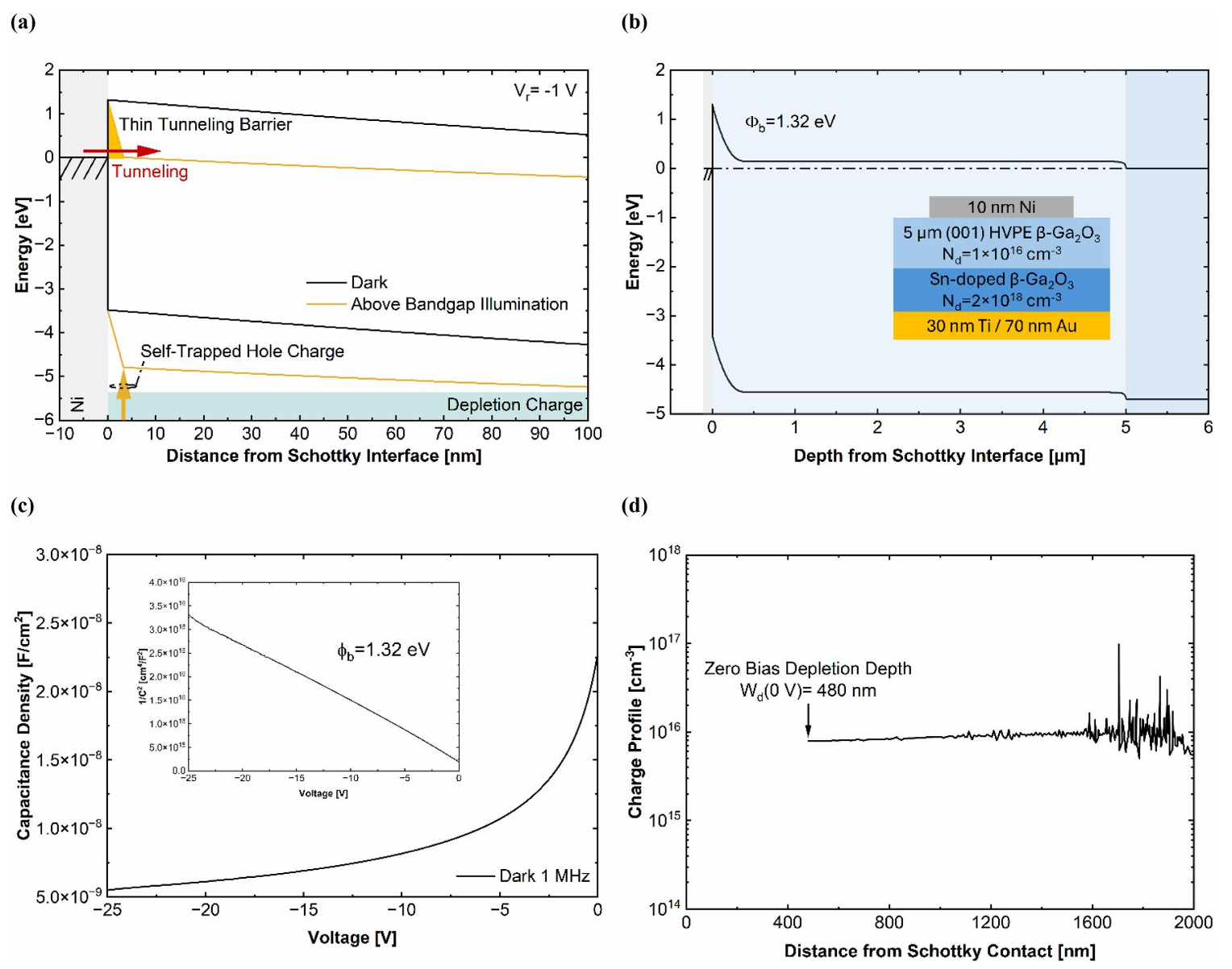
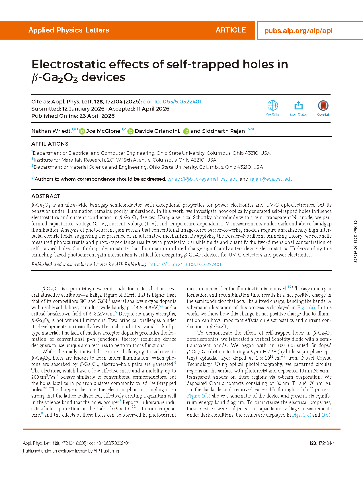
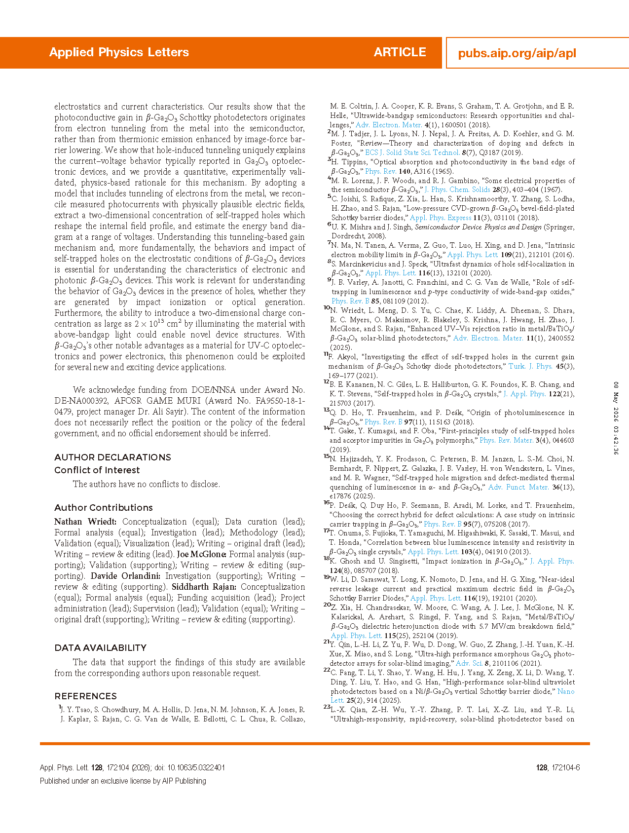
Fig. 1 (a) A schematic illustration of the mechanism by which self-trapped holes bend the conduction and valence bands in a Schottky diode and (b) equilibrium band diagram of the device under test (inset: schematic diagram), as well as (c) the dark C–V curve (inset: plot of 1/C2, showing a built-in voltage of 1.32 eV), and (d) the extracted doping profile (Nd=1×1016 cm-3).
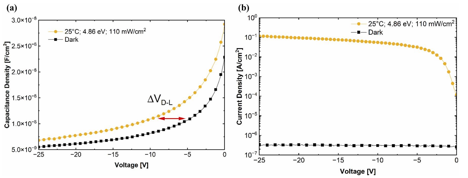
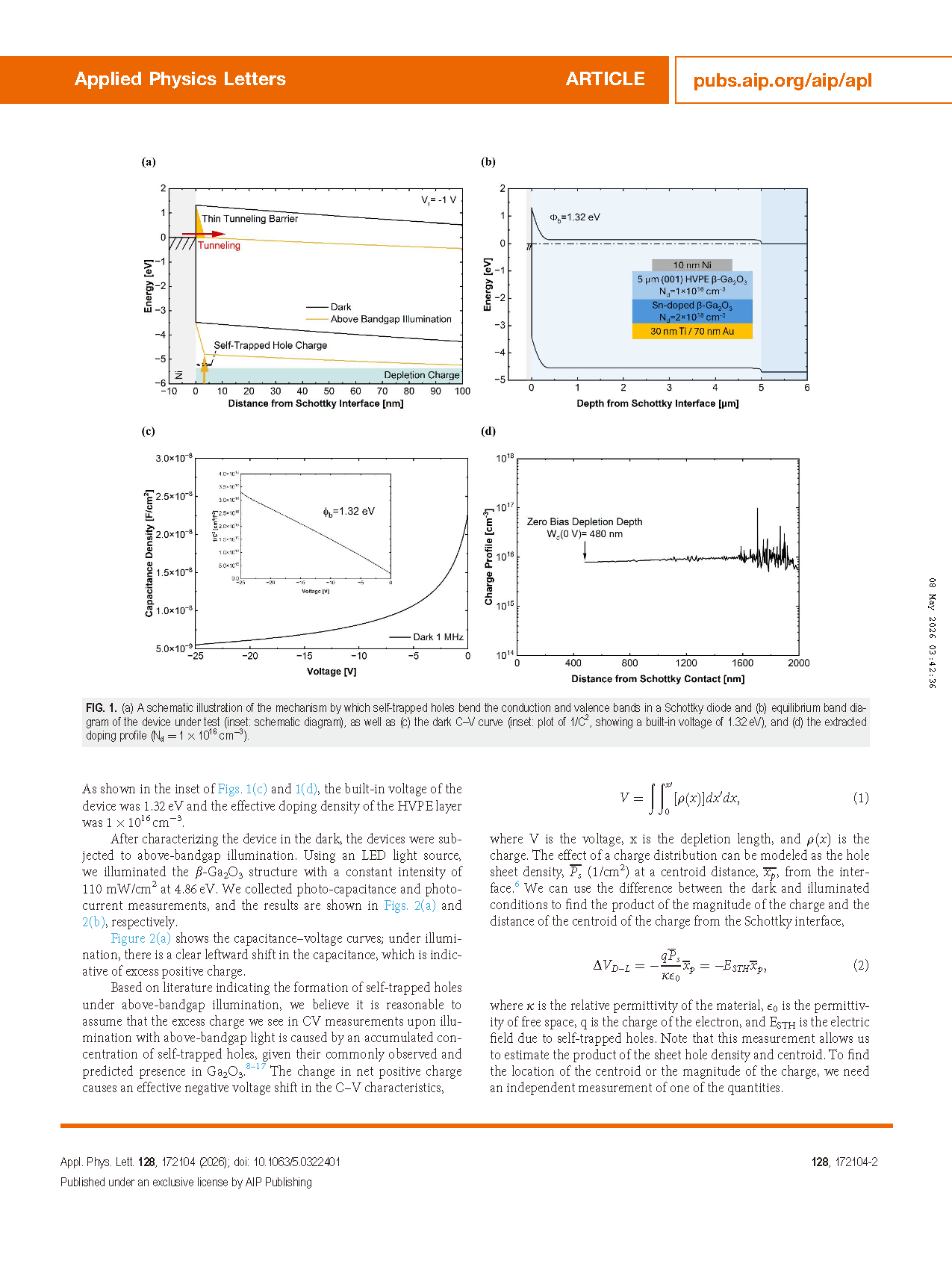
Figure 2. (a) Capacitance (1 MHz) and (b) I–V measurements collected in both dark and illuminated (4.86 eV; 110 mW/cm2) conditions.
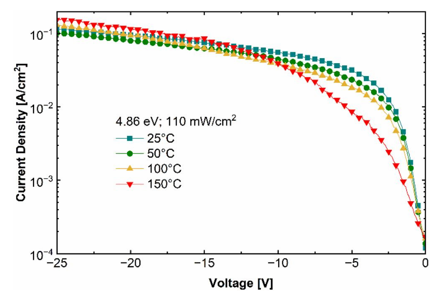
Figure 3. Temperature dependent I-V curves under 110 mW/cm2 of 4.86 eV CW illumination.
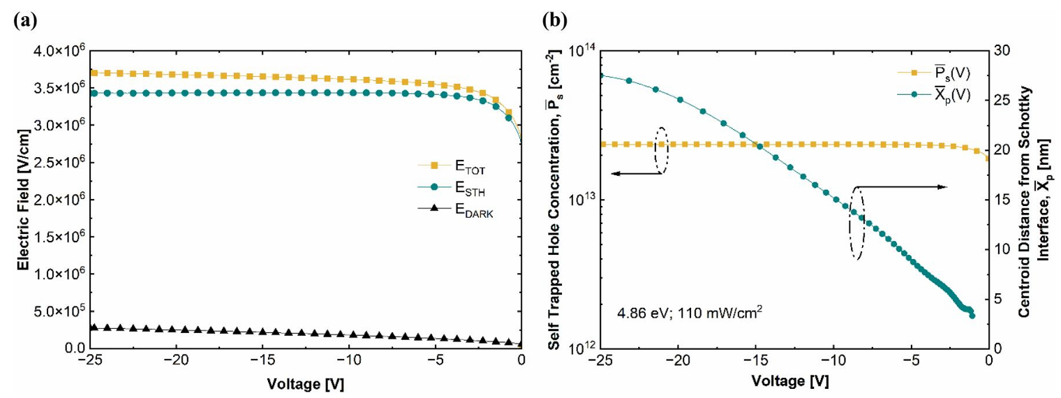
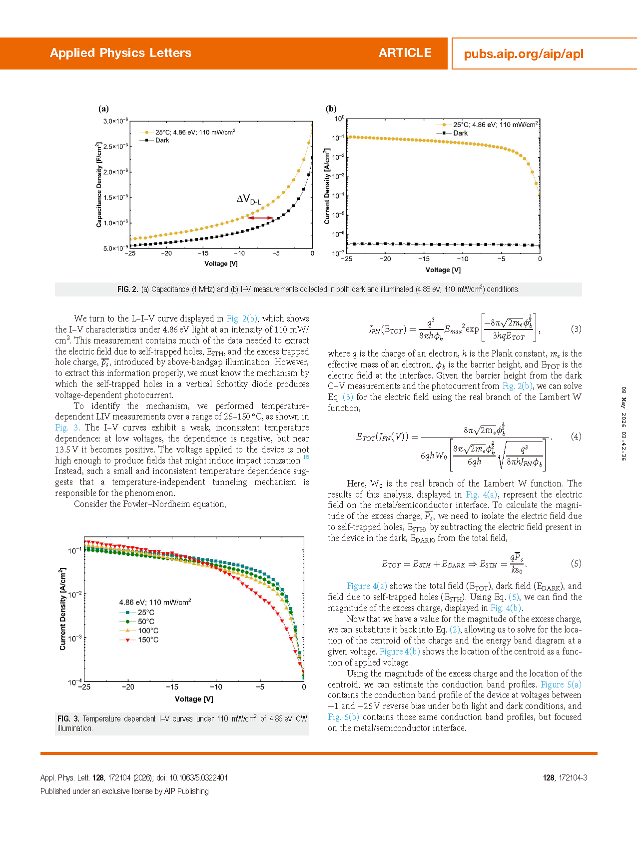
Figure 4. Plot of (a) the electric fields observed, extracted from the light-induced current and (b) the magnitude and location of light-induced excess charge with respect to voltage.
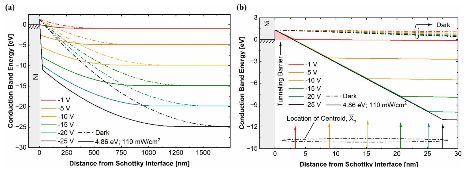
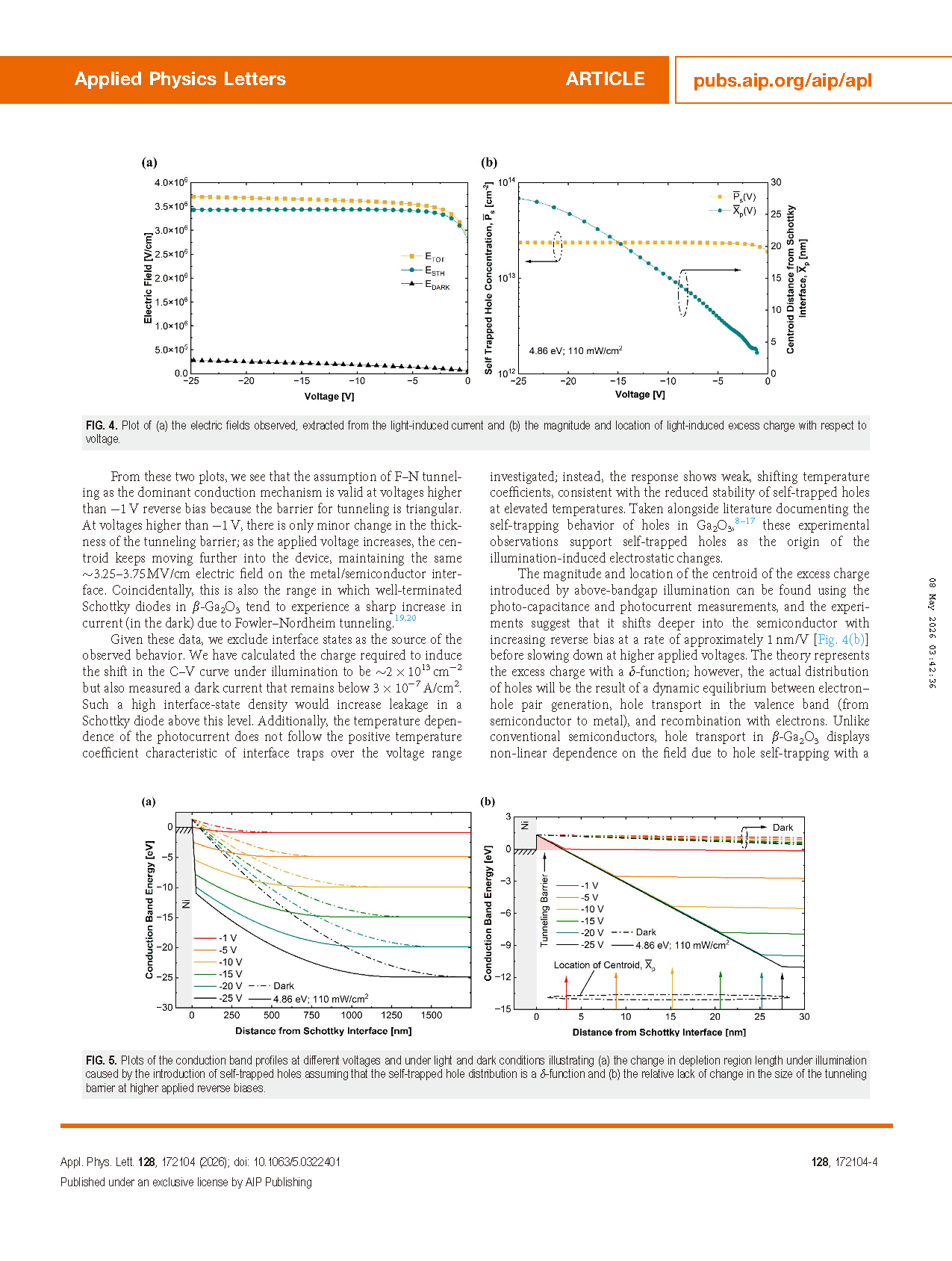
Figure 5. Plots of the conduction band profiles at different voltages and under light and dark conditions illustrating (a) the change in depletion region length under illumination caused by the introduction of self-trapped holes assuming that the self-trapped hole distribution is a δ-function and (b) the relative lack of change in the size of the tunneling barrier at higher applied reverse biases.
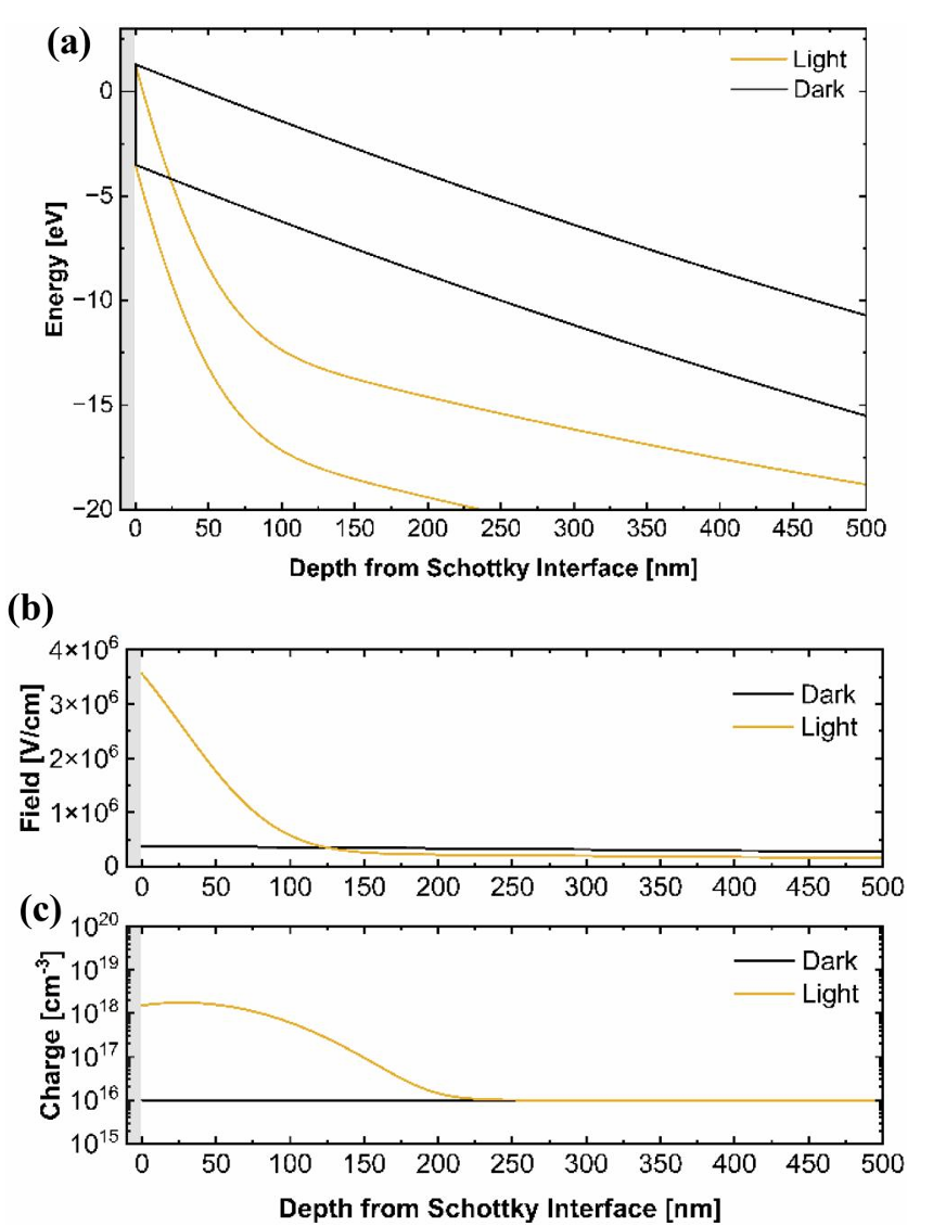
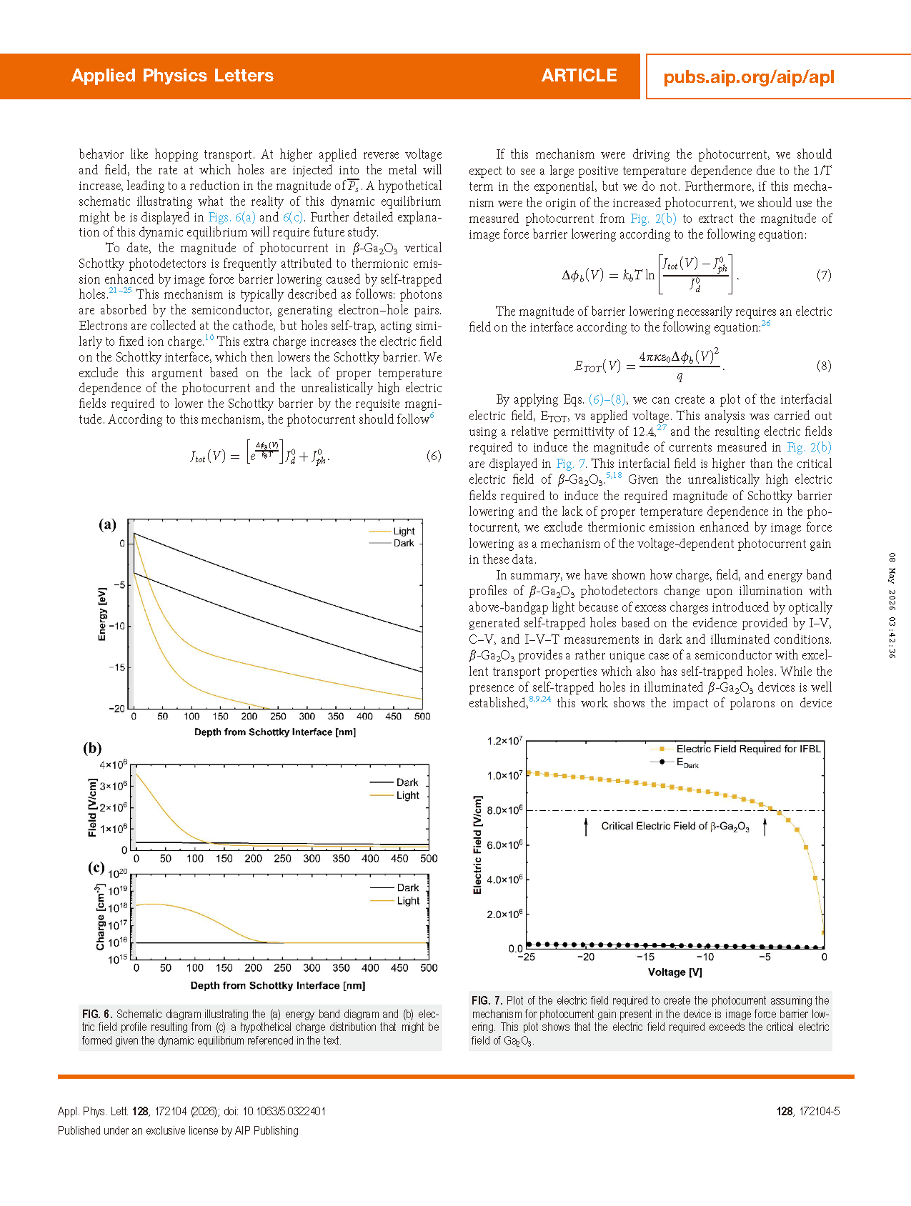
Figure 6 Schematic diagram illustrating the (a) energy band diagram and (b) electric field profile resulting from (c) a hypothetical charge distribution that might be formed given the dynamic equilibrium referenced in the text.
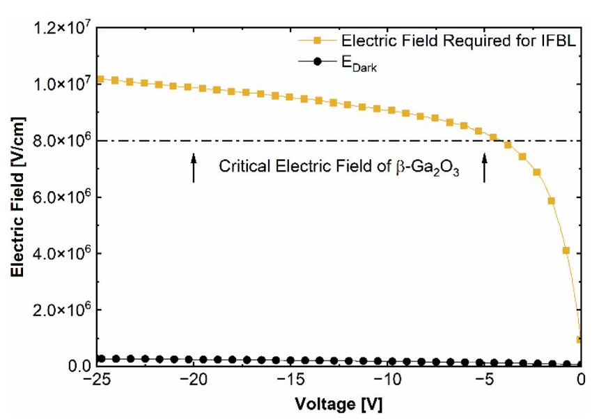
Figure 7. Plot of the electric field required to create the photocurrent assuming the mechanism for photocurrent gain present in the device is image force barrier lowering. This plot shows that the electric field required exceeds the critical electric field of Ga2O3.
DOI:
doi.org/10.1063/5.0322401