Paper Sharing
【Domestic Papers】Exploring thermal transport in β-Ga₂O₃ films: The effect of epitaxial growth parameters
日期:2026-05-08阅读:59
Researchers from Shandong University have published a dissertation titled “Exploring thermal transport in β‑Ga₂O₃ films: The effect of epitaxial growth parameters” in Ceramics International.
Background
β‑Ga₂O₃ is a promising ultra-wide bandgap semiconductor for next-generation power electronic devices, but its low intrinsic thermal conductivity and obvious anisotropy lead to serious heat dissipation issues, which have become a key bottleneck for its practical application. Epitaxial growth is a core method to obtain high-quality β‑Ga₂O₃ films. However, key parameters such as growth temperature, pressure, and thickness can significantly introduce grain defects, oxygen vacancies, and interface loss, which strongly scatter phonons and reduce thermal conductivity. Most existing studies focus on crystal and optoelectronic properties, while the regulation mechanism of thermal transport in PLD-prepared β‑Ga₂O₃ films is still unclear, and a systematic correlation among growth parameters, microstructure, and thermal conductivity is lacking.
Abstract
Gallium oxide (β‑Ga₂O₃) has emerged as a promising ultrawide-bandgap semiconductor for the next-generation high-performance micro-nano electronic devices. However, its inherently and highly anisotropic thermal conductivity poses a significant challenge for heat dissipation, which is critically influenced by the microstructural defects introduced during the film growth. This work systematically investigates the effects of key growth parameters (temperature, pressure and film thickness) on the thermal conductivity of β‑Ga₂O₃ films epitaxially grown on c-plane sapphire via pulsed laser deposition. The thermal conductivity is characterized using the differential 3ω method. The results reveal that all three parameters exert a profound influence. Specifically, elevating the growth temperature from 650 ℃ to 850 ℃ enhances the film thermal conductivity by approximately 140%, reaching 5.18 W·m⁻¹·K⁻¹. This improvement is mechanistically linked to increased grain size and reduced point defect density, both of which weaken phonon scattering at grain boundaries and by vacancies. Furthermore, optimizing the growth pressure is shown to be an effective strategy for significantly improving thermal conductivity, likely by modifying adatom mobility and defect. Additionally, the thermal conductivity increases substantially from 2.37 W·m⁻¹·K⁻¹ to 4.04 W·m⁻¹·K⁻¹ as the thickness increases from 136 nm to 674 nm, demonstrating a size effect where the film thickness confines the mean free path of the dominant heat carrying phonons. Moreover, the thermal resistance is deduced to be 4.31 ×10⁻⁸ m²·K·W⁻¹. This study establishes a clear microstructure-thermal property relationship governed by phonon scattering mechanisms and provides crucial guidance for the design of growth parameters to engineer the thermal transport properties of β‑Ga₂O₃ films for advanced device applications.
Highlights
The thermal conductivity of PLD-grown β‑Ga₂O₃ films is measured using 3ω method.
The thermal conductivity of β‑Ga₂O₃ film can be significantly enhanced by optimizing epitaxial growth temperature and pressure.
The thermal conductivity of β‑Ga₂O₃ film grown at 850 ℃ is 5.18 W・m⁻¹・K⁻¹, which is ~2.4 times of that grown at 650 ℃.
A strong thickness-dependent thermal conductivity is observed in β‑Ga₂O₃ films.
Phonon-boundary scattering and phonon-vacancy scattering are identified as the key mechanisms through which growth parameters govern the thermal conductivity of β‑Ga₂O₃ film.
Conclusion
In this work, the thermal conductivity of β‑Ga₂O₃ films epitaxially grown on c-plane sapphire via pulsed laser deposition (PLD) is systematically investigated using the differential 3ω method. The work establishes a clear and quantitative relationship between key growth parameters (temperature, pressure and film thickness), and the resulting thermal transport properties, elucidating the underlying phonon scattering mechanisms. A strong dependence of thermal conductivity on growth temperature is observed, with the value increasing by approximately 140% (from ~2.20 to 5.18 W·m⁻¹·K⁻¹) as the temperature is raised from 650 ℃ to 850 ℃. This enhancement is primarily attributed to the increased grain size and reduces point defect concentration, both of which diminish phonon scattering at grain boundaries and by vacancies, which is verified by the BTE-calculated phonon scattering rates results. Furthermore, growth pressure is identified as a critical non‑monotonic control parameter. Thermal conductivity exhibits a “V-shaped” trend within the investigated pressure range (4.5 to 8.5 mTorr), with films grown at 4.5 and 8.5 mTorr showing significantly higher conductivity than those at an intermediate pressure of 6.5 mTorr. This behavior is linked to pressure‑dependent adatom mobility and defect incorporation kinetics during PLD growth. A pronounced thickness‑dependent size effect was confirmed, where thermal conductivity increased monotonically from 2.37 to 4.04 W·m⁻¹·K⁻¹ as the film thickness increased from 136 to 674 nm. This trend is governed by the progressive relaxation of boundary scattering for long MFP phonons as the film thickness surpasses their characteristic scattering length. By analyzing the thickness-dependent thermal conductivity, the total thermal resistance is extracted to be 4.31 ×10⁻⁸ m²·K·W⁻¹, a value indicative of the phonon mismatch and interfacial imperfections inherent to the heteroepitaxial system. The findings of this work underscore that the thermal conductivity of β‑Ga₂O₃ films is not an intrinsic material property but is decisively governed by the synthesis conditions. By providing a mechanistic framework that connects growth parameters (temperature, pressure and thickness) to microstructural features and dominant phonon scattering processes, this work offers crucial insights and practical guidance for the design of growth protocols. Optimizing these parameters presents a direct pathway to engineer the thermal performance of β‑Ga₂O₃ films, which is essential for improving heat dissipation and ensuring the reliability of next-generation high-power electronic devices.
Project Support
This work was supported by the Natural Science Foundation of Shandong Province (No. ZR2025ZD32), the Shenzhen Science and Technology Program (Nos. JCYJ20240813101231040, JCYJ20250604124217023), Guangdong Basic and Applied Basic Research Foundation (Nos. 2025A1515012590), National Natural Science Foundation of China (No. 52576077), and The Youth Innovation Technology Support Program of Higher Education Institutions of Shandong Province (No. 2023KJ003).
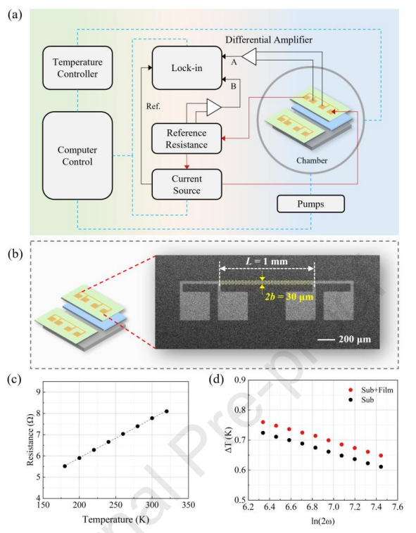
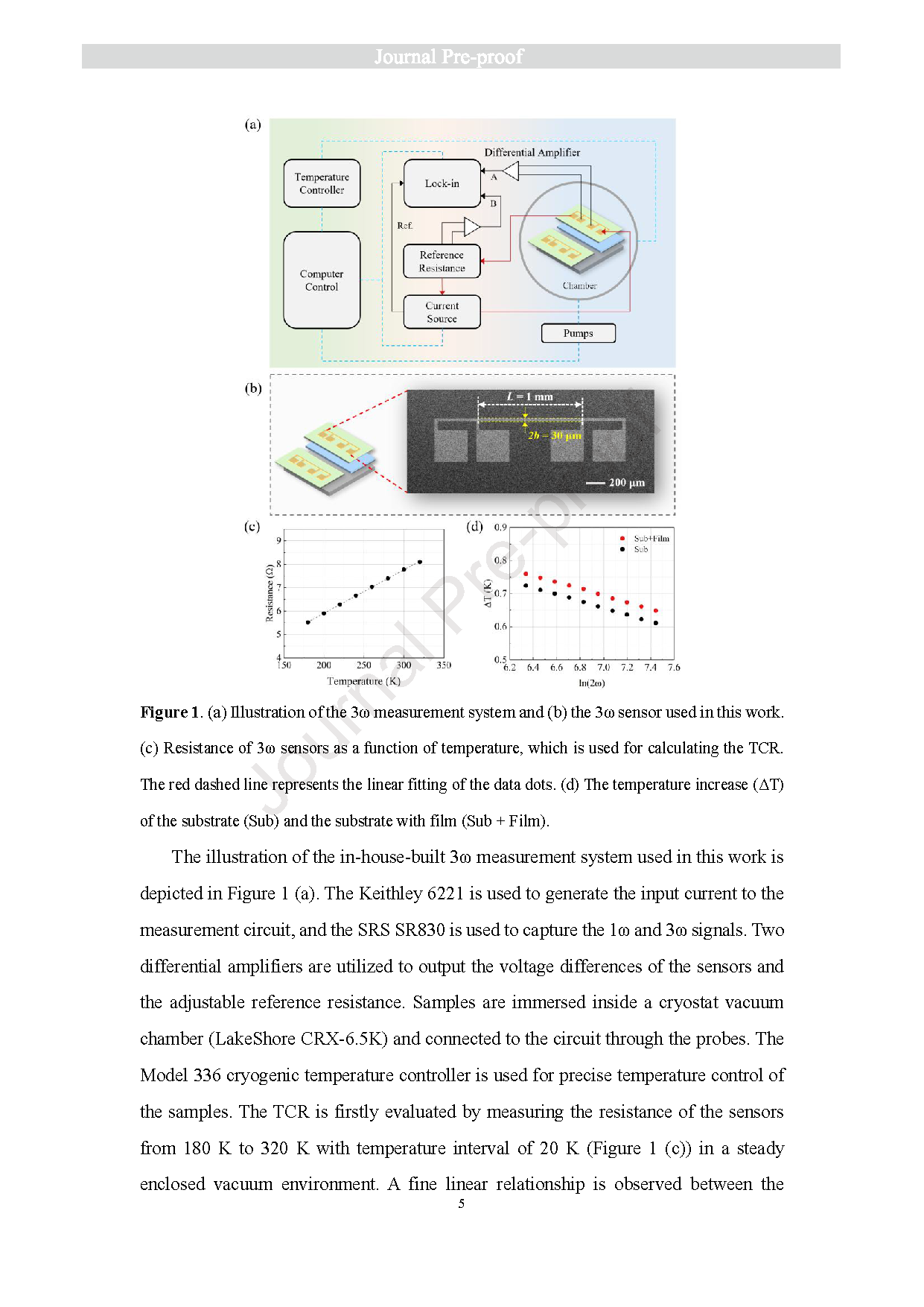
Figure 1. (a) Illustration of the 3ω measurement system and (b) the 3ω sensor used in this work. (c) Resistance of 3ω sensors as a function of temperature, which is used for calculating the TCR. The red dashed line represents the linear fitting of the data dots. (d) The temperature increase (ΔT) of the substrate (Sub) and the substrate with film (Sub + Film).
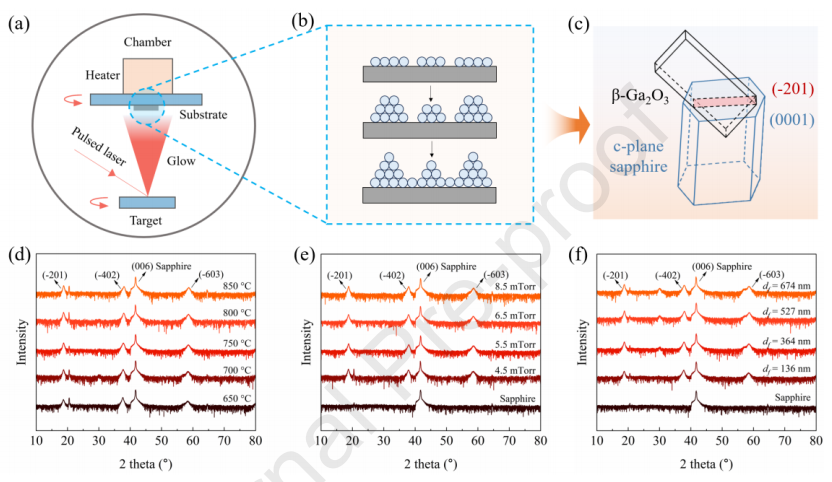
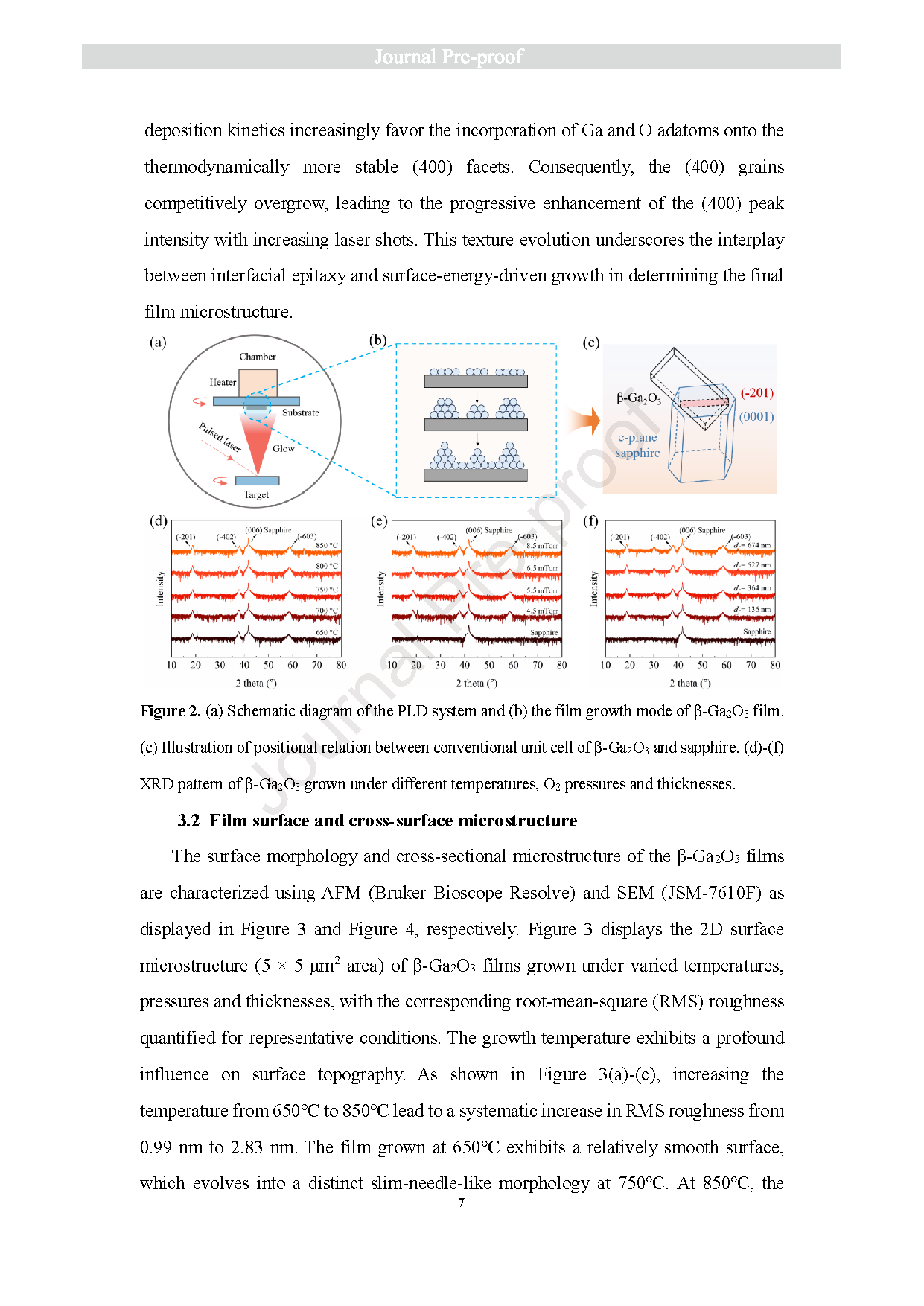
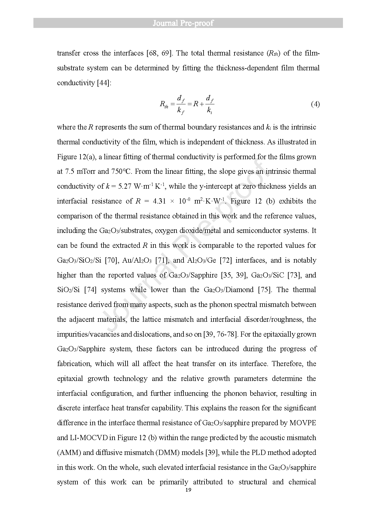
Figure 2. (a) Schematic diagram of the PLD system and (b) the film growth mode of β‑Ga₂O₃ film. (c) Illustration of positional relation between conventional unit cell of β‑Ga₂O₃ and sapphire. (d)-(f) XRD pattern of β‑Ga₂O₃ grown under different temperatures, O₂ pressures and thicknesses.
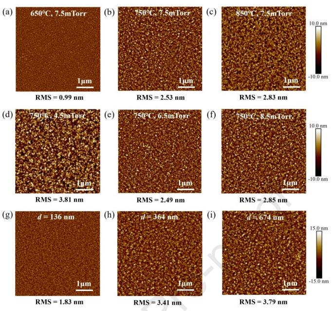
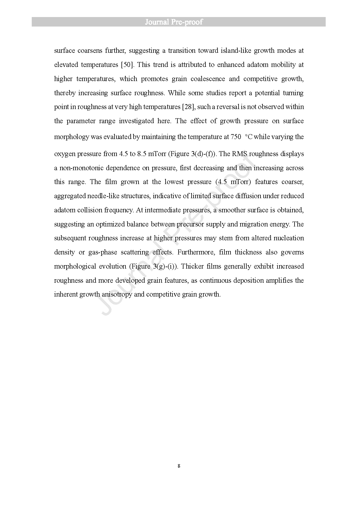
Figure 3. (a)-(c) AFM images of the film surface grown under different temperatures. (d)-(f) AFM images of the film surface grown under different pressures. (h)-(g) AFM images of the film surface with different thicknesses.
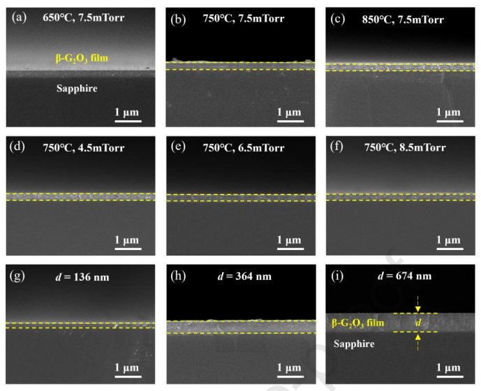
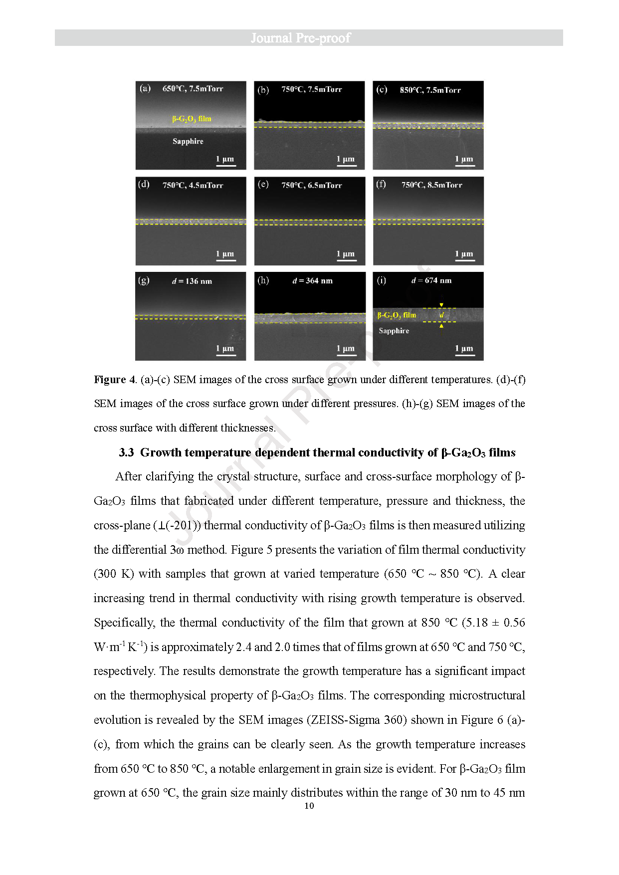
Figure 4. (a)-(c) SEM images of the cross surface grown under different temperatures. (d)-(f) SEM images of the cross surface grown under different pressures. (h)-(g) SEM images of the cross surface with different thicknesses.
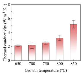
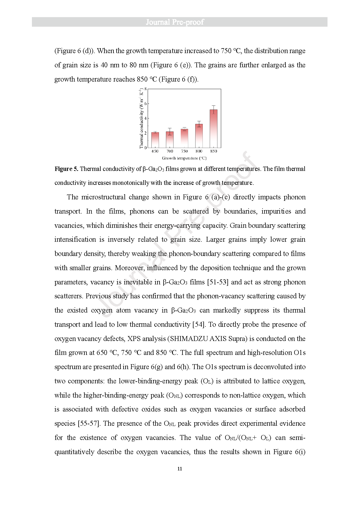
Figure 5. Thermal conductivity of β‑Ga₂O₃ films grown at different temperatures. The film thermal conductivity increases monotonically with the increase of growth temperature.
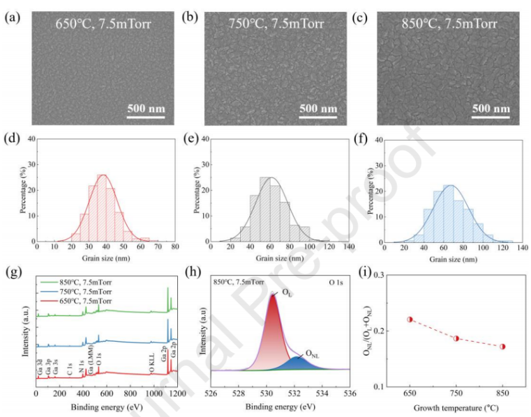
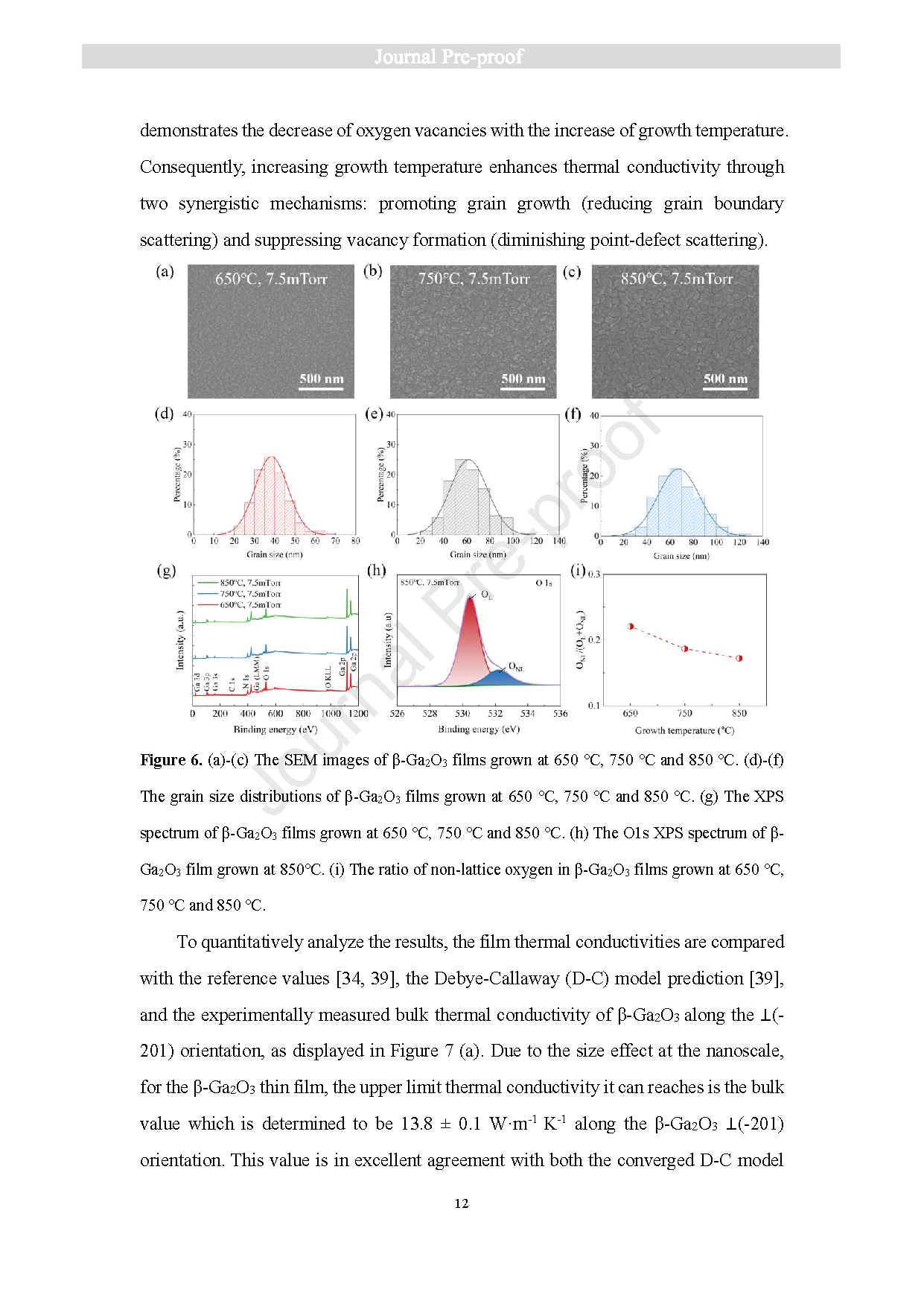
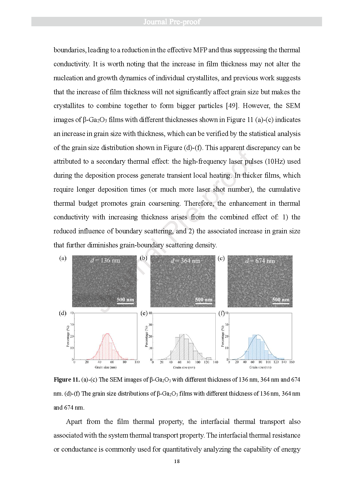
Figure 6. (a)-(c) The SEM images of β‑Ga₂O₃ films grown at 650 ℃, 750 ℃ and 850 ℃. (d)-(f) The grain size distributions of β‑Ga₂O₃ films grown at 650 ℃, 750 ℃ and 850 ℃. (g) The XPS spectrum of β‑Ga₂O₃ films grown at 650 ℃, 750 ℃ and 850 ℃. (h) The O 1s XPS spectrum of β‑Ga₂O₃ film grown at 850 ℃. (i) The ratio of non-lattice oxygen in β‑Ga₂O₃ films grown at 650 ℃, 750 ℃ and 850 ℃.
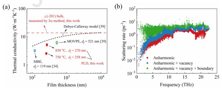
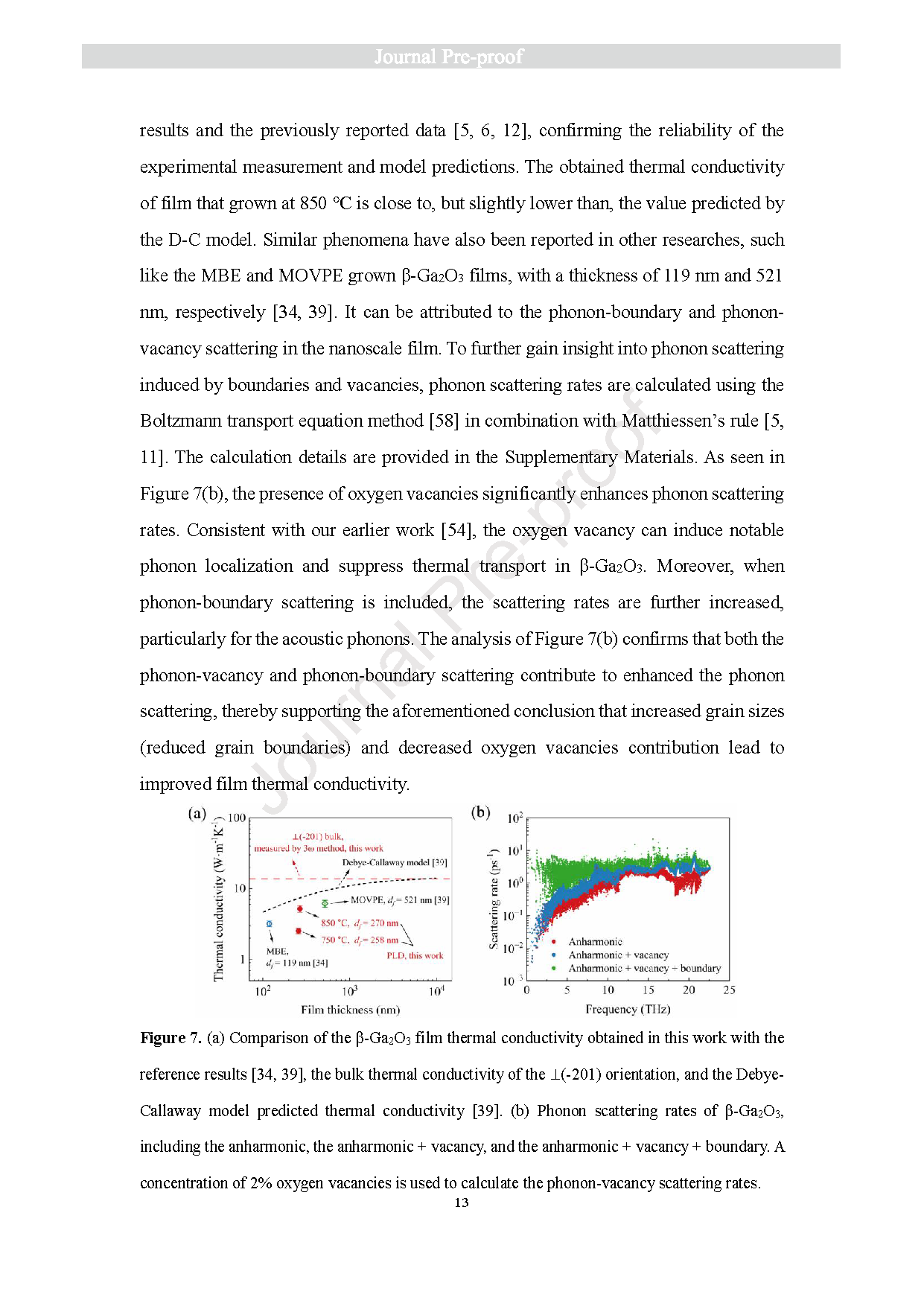
Figure 7. (a) Comparison of the β‑Ga₂O₃ film thermal conductivity obtained in this work with the reference results [34, 39], the bulk thermal conductivity of the ⊥(-201) orientation, and the Debye-Callaway model predicted thermal conductivity [39]. (b) Phonon scattering rates of β‑Ga₂O₃, including the anharmonic, the anharmonic + vacancy, and the anharmonic + vacancy + boundary. A concentration of 2% oxygen vacancies is used to calculate the phonon-vacancy scattering rates.
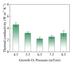
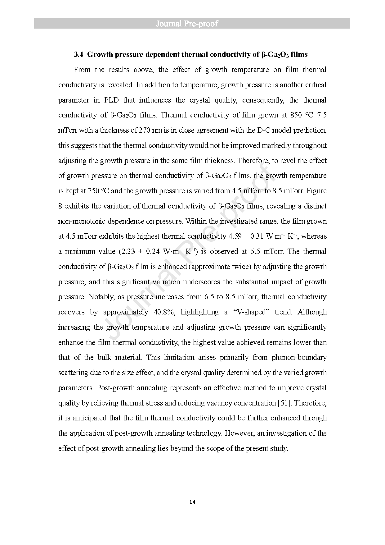
Figure 8. Thermal conductivity of β‑Ga₂O₃ films grown at different pressures with a fixed temperature of 750 °C. A “V-shaped” film thermal conductivity appears with the increase of growth pressure.
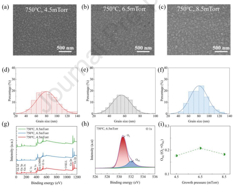
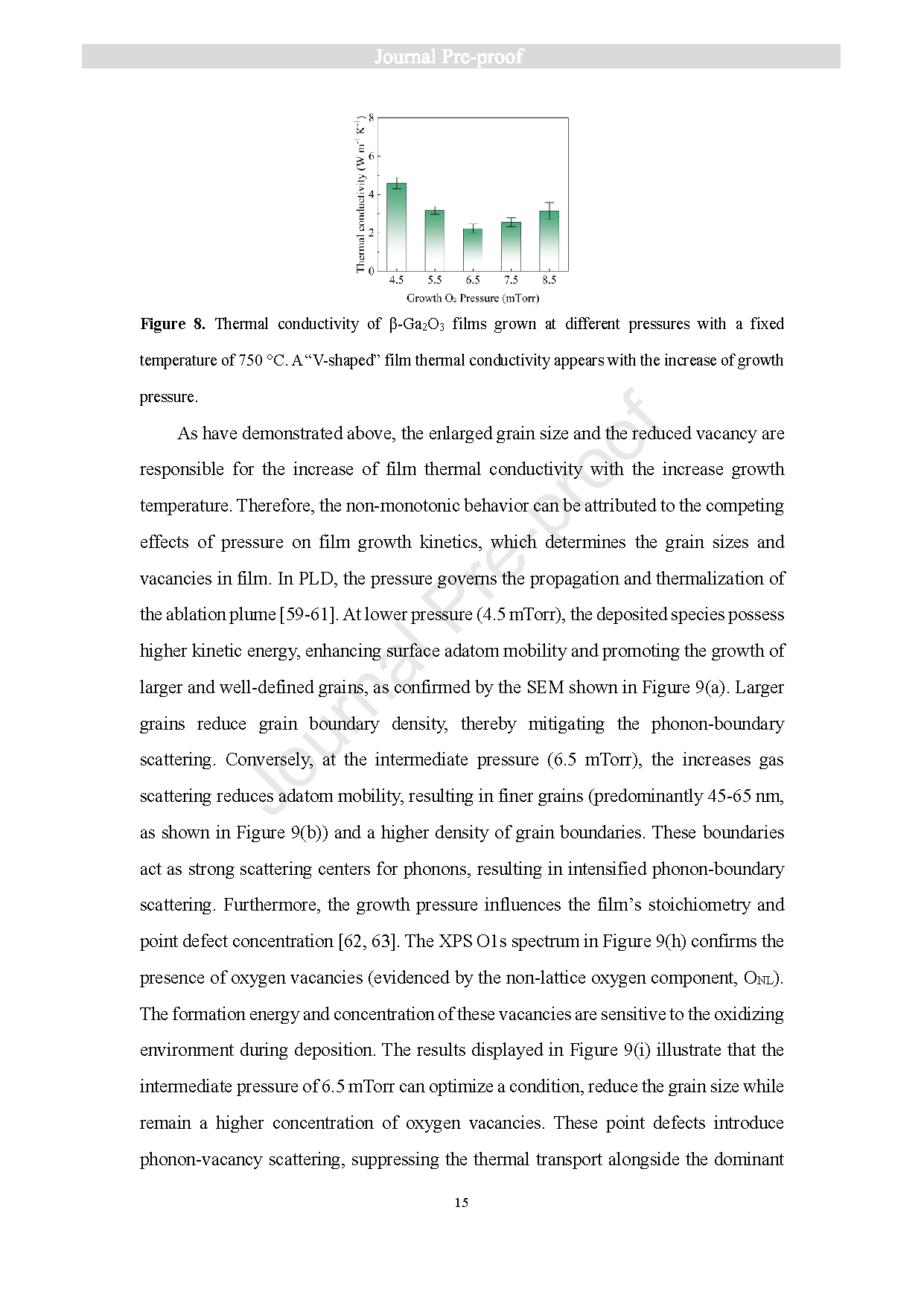
Figure 9. (a)-(c) SEM images of β‑Ga₂O₃ films grown at 4.5mTorr, 6.5mTorr and 8.5mTorr. (d)-(f) The grain size distributions of β‑Ga₂O₃ films grown at 4.5mTorr, 6.5mTorr and 8.5mTorr. (g) The XPS spectrum of β‑Ga₂O₃ films grown at 4.5mTorr, 6.5mTorr and 8.5mTorr. (h) The O1s XPS spectrum of β‑Ga₂O₃ film grown at 6.5mTorr. (i) The ratio of non-lattice O (ONL) in β‑Ga₂O₃ films grown at 4.5mTorr, 6.5mTorr and 8.5mTorr.
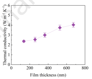
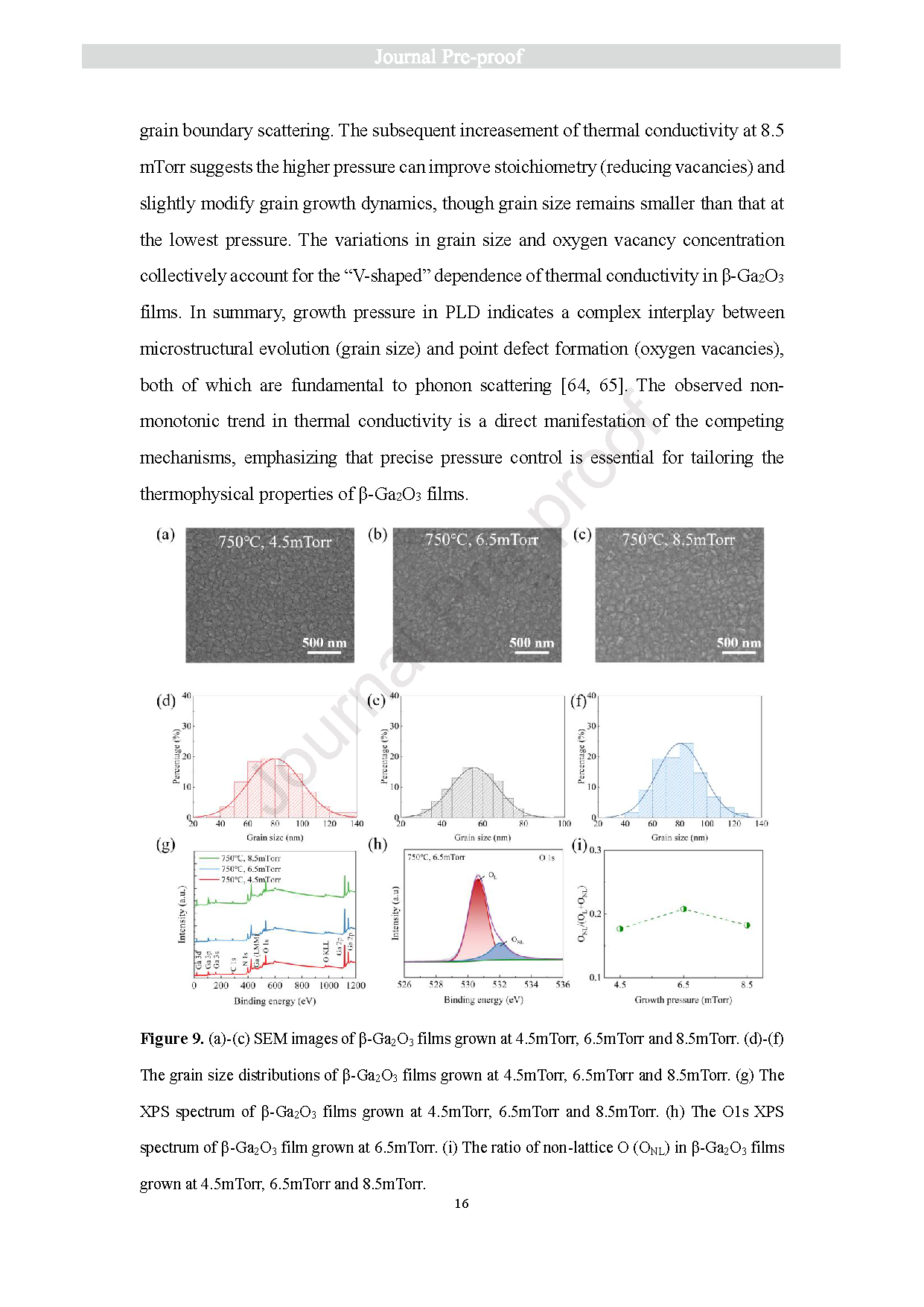
Figure 10. Thermal conductivity of β‑Ga₂O₃ films with different thicknesses with a fixed growth condition of 750 °C_7.5 mTorr. An obvious size effect of β‑Ga₂O₃ film thermal conductivity can be detected.
DOI:
doi.org/10.1016/j.ceramint.2026.04.339