Paper Sharing
【Member Papers】Tunable electronic properties of κ-(Al, In)₂O₃/Ga₂O₃ digital alloys via superlattice design
日期:2026-04-03阅读:28
Researchers from the Hong Kong University of Science and Technology (Guangzhou) have published a dissertation titled "Tunable electronic properties of κ-(Al, In)2O3/Ga2O3 digital alloys via superlattice design" in Journal of Applied Physics.
Project Support
This work was supported by the C. K. Tan start-up fund from the Hong Kong University of Science and Technology (Guangzhou), the Guangzhou Municipal Science and Technology Project (Nos. 2023A03J0003, 2023A03J0013, 2023A04J0310, and 2023A03J0152), the Department of Education of Guangdong Province (No. 2024ZDZX1005), and the State Administration of Foreign Experts Affairs (No. Y20240005). The authors also acknowledge financial support from the Shenzhen Science and Technology Innovation Commission (No. 20231115111658002). This work was supported by the Materials Characterization and Preparation Facility (MCPF) and the Green Materials Laboratory at the Hong Kong University of Science and Technology (Guangzhou). The work was also supported by the Matching Funding for Selected Talent of National Programs (No. CZ118SC24007), National Major Talent Project (No. CZ118SC25005), and Excellent Young Scientists Fund (overseas): Nos. RK118QN24006 and RK118QN25006. The numerical calculations in this paper have been done using computational resources from Guangzhou Tanoxi Company.
Background
Gallium oxide (Ga2O3) has emerged as a highly promising wide-bandgap semiconductor due to its exceptional material properties, such as a large breakdown field (∼8 MV/cm) and tunable bandgaps across polymorphs. Among its various phases, the metastable orthorhombic phase (κ-Ga2O3) has garnered significant attention due to its high spontaneous electrical polarization property, which surpasses that of conventional III-nitrides, such as AlN and GaN. This property enables polarization-induced doping at heterointerfaces, facilitating the formation of two-dimensional electron gases (2DEGs) without extrinsic dopants, makes it suitable for high-electron-mobility transistors (HEMTs) and quantum-well infrared photodetectors (QWIPs).
In addition, forming κ-(AlxGa1−x)2O3 and κ-(InxGa1−x)2O3 alloys would be a promising strategy to adjust the material properties and modify the polarization differences to increase localize 2DEGs with higher sheet charge carrier densities. Tahara et al. demonstrated the ε-(AlxGa1−x)2O3 grown by mist chemical vapor deposition. Nishinaka et al. reported the ε-(InxGa1−x)2O3 on c-plane sapphire for bandgap tuning. The stabilized pure-phase κ-(AlxGa1−x)2O3 and κ-(InxGa1−x)2O3 thin film was also revealed by pulsed laser deposition (PLD). However, experimental feasibility remains a critical challenge at high Al or In concentrations in the random alloy, particularly regarding phase separation and high threading dislocation densities. Furthermore, controlling the phase stability between the metastable κ-polymorph and the competing α-phase or the thermodynamically stable β-phase presents a significant hurdle in bulk heteroepitaxy. Therefore, it is necessary to find an alternative strategy to enhance crystalline and interface quality.
Abstract
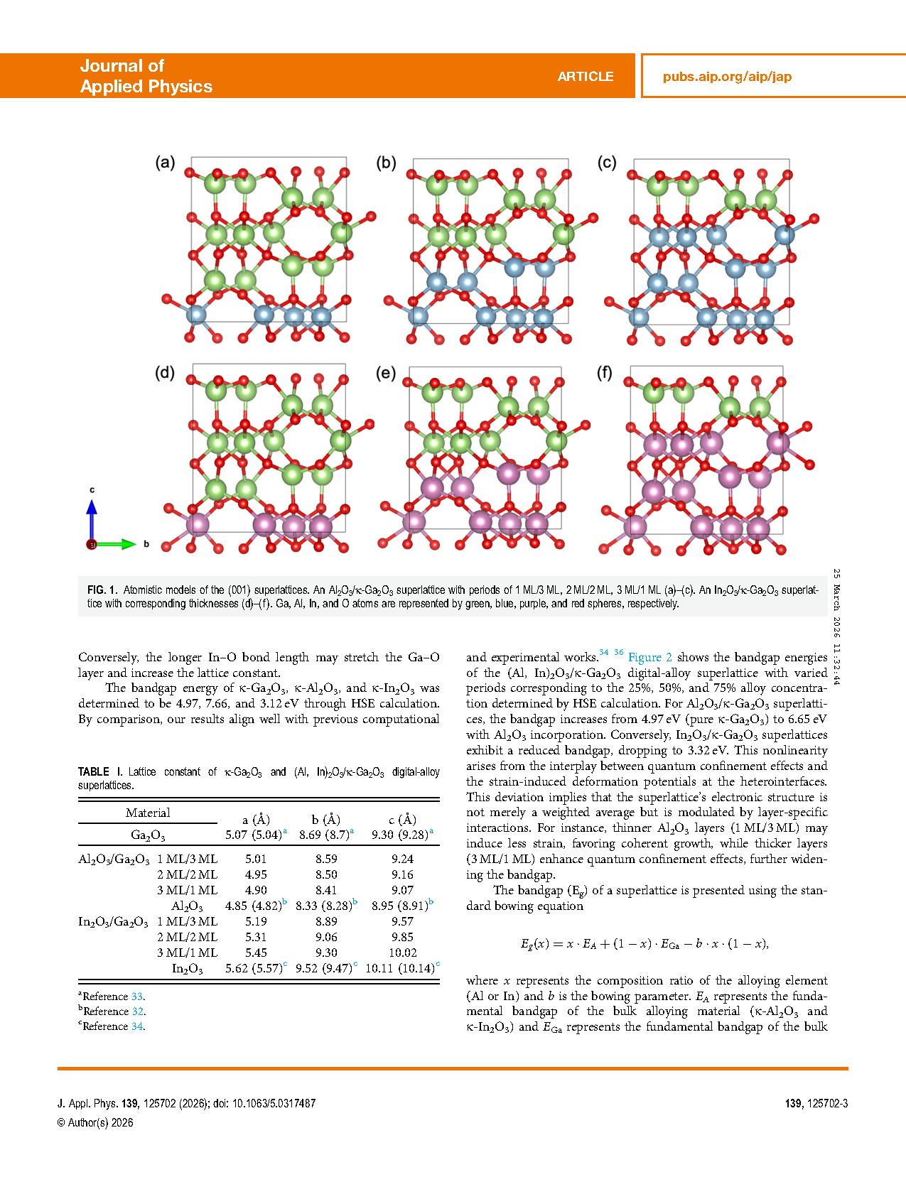
κ-Ga2O3-based digital-alloy superlattices offer a promising alternative to traditional random alloys for high performance heterostructure devices. Using density functional theory, we model (Al2O3/κ-Ga2O3) and (In2O3/κ-Ga2O3) superlattices with varying monolayer (ML) thicknesses (1 ML/3 ML, 2 ML/2 ML, and 3 ML/1 ML). Our calculations reveal precise tuning of lattice parameters and bandgaps dependent on layer thickness. The incorporation of Al2O3 introduces tensile strain and widens bandgap up to 6.65 eV, while In2O3-rich structures exhibit compressive strain with bandgap reduction down to 3.32 eV. Element-projected band structures confirm quantum confinement effects and interfacial contributions to electronic states. Notably, intersubband transition energies are controllable via ML thickness, enabling absorption in the telecom-compatible wavelength range (∼1.55 μm). Band alignment analysis reveals significant conduction band offsets (up to 3.71 eV for Al2O3/Ga2O3), which is vital for polarization-induced 2DEG (two-dimensional electron gas) formation. This work demonstrates the feasibility of κ-Ga2O3 digital-alloy superlattices for tailored high-electron-mobility transistors and quantum-well infrared photodetectors.
Conclusion
In summary, we performed first-principles DFT calculations to investigate the structural and electronic properties of a κ-Ga2O3-based digital-alloy superlattice. We demonstrated that the bandgap can be tuned over a wide range (3.32–6.65 eV) by varying the ML thickness of Al2O3 and In2O3 insertions, overcoming the phase separation challenges typical of random ternary alloys. The calculations reveal that intersubband transition energies can be engineered to target the telecommunication wavelength (1.55 μm). Furthermore, the adjustable conduction band offset (up to 3.71 eV) in Al2O3/κ-Ga2O3 systems highlights their potential for high confinement 2DEGs in HEMT application. These results establish κ-phase digital alloys as a viable and flexible platform for next-generation oxide electronics and optoelectronics.
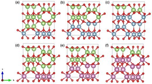
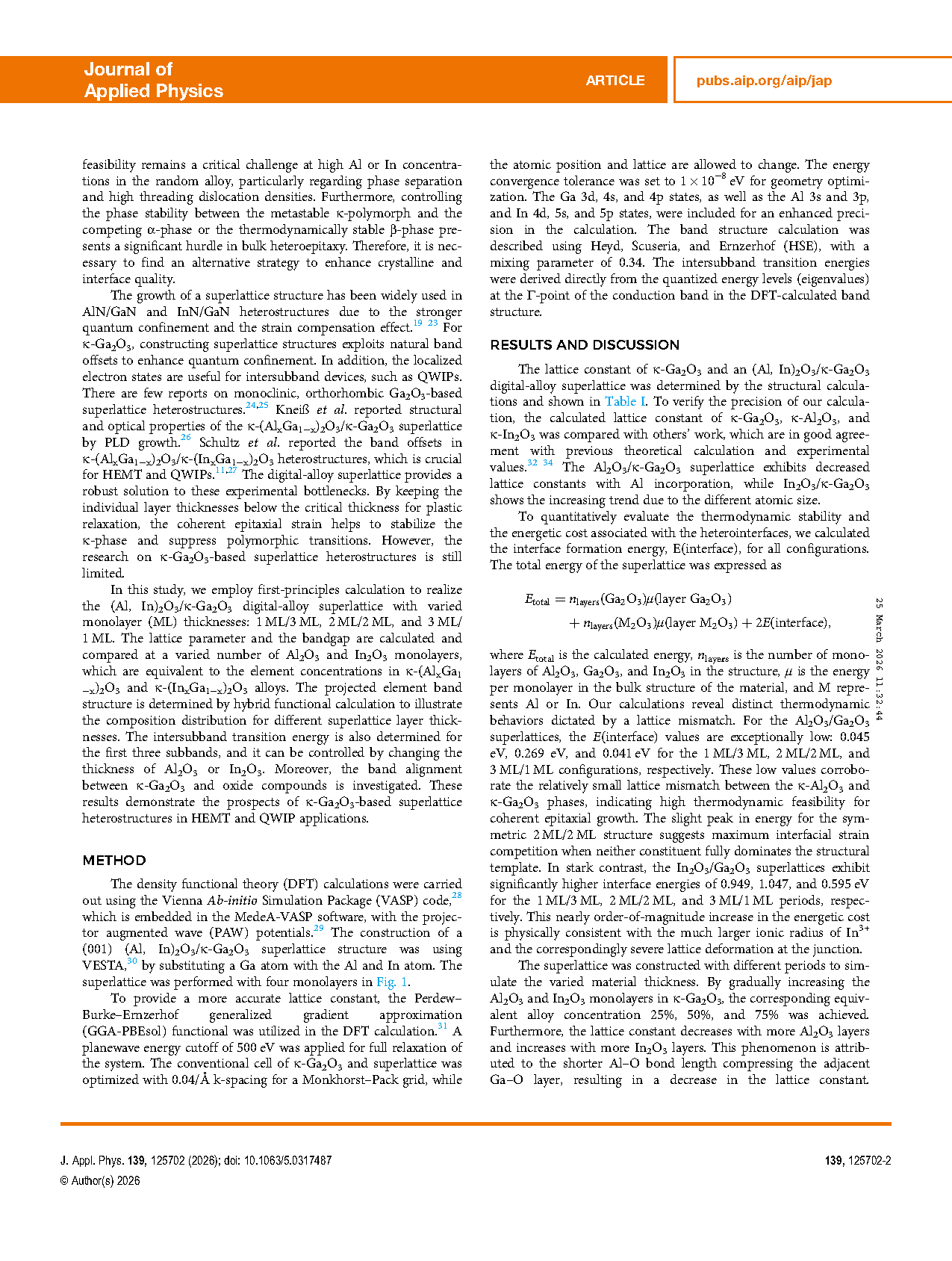
FIG. 1. Atomistic models of the (001) superlattices. An Al2O3/κ-Ga2O3 superlattice with periods of 1 ML/3 ML, 2 ML/2 ML, 3 ML/1 ML (a)–(c). An In2O3/κ-Ga2O3 superlattice with corresponding thicknesses (d)–(f). Ga, Al, In, and O atoms are represented by green, blue, purple, and red spheres, respectively.
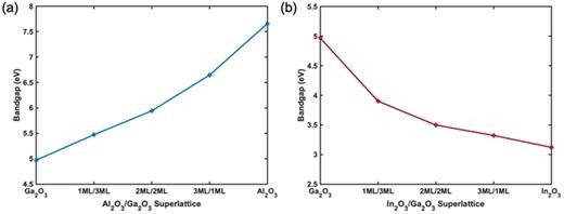
FIG. 2. Bandgap energy of a (001) Al2O3/κ-Ga2O3 superlattice (a) and a (001) In2O3/κ-Ga2O3 superlattice (b).
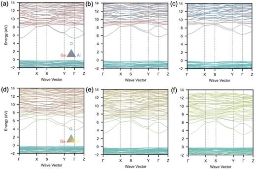
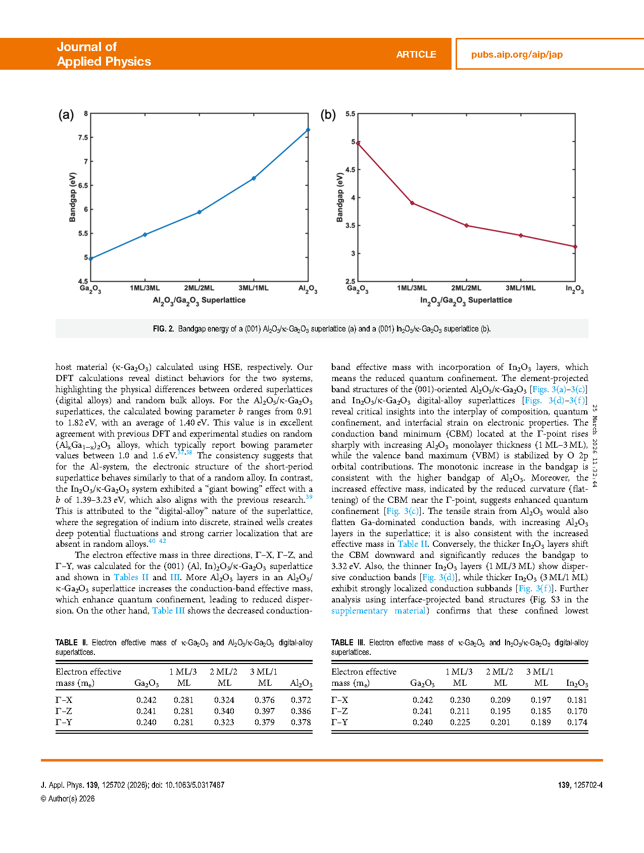
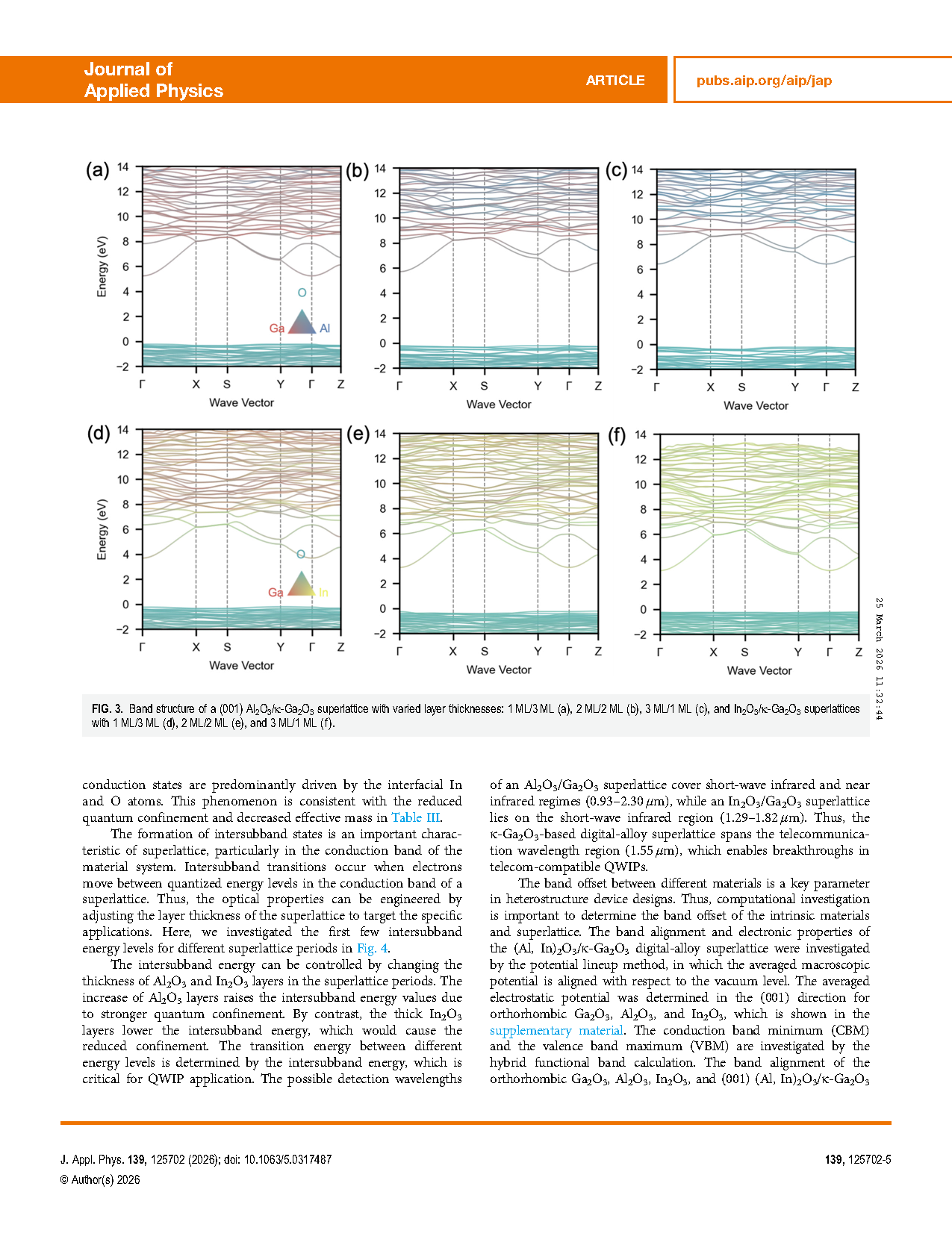
FIG. 3. Band structure of a (001) Al2O3/κ-Ga2O3 superlattice with varied layer thicknesses: 1 ML/3 ML (a), 2 ML/2 ML (b), 3 ML/1 ML (c), and In2O3/κ-Ga2O3 superlattices with 1 ML/3 ML (d), 2 ML/2 ML (e), and 3 ML/1 ML (f).
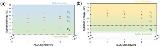
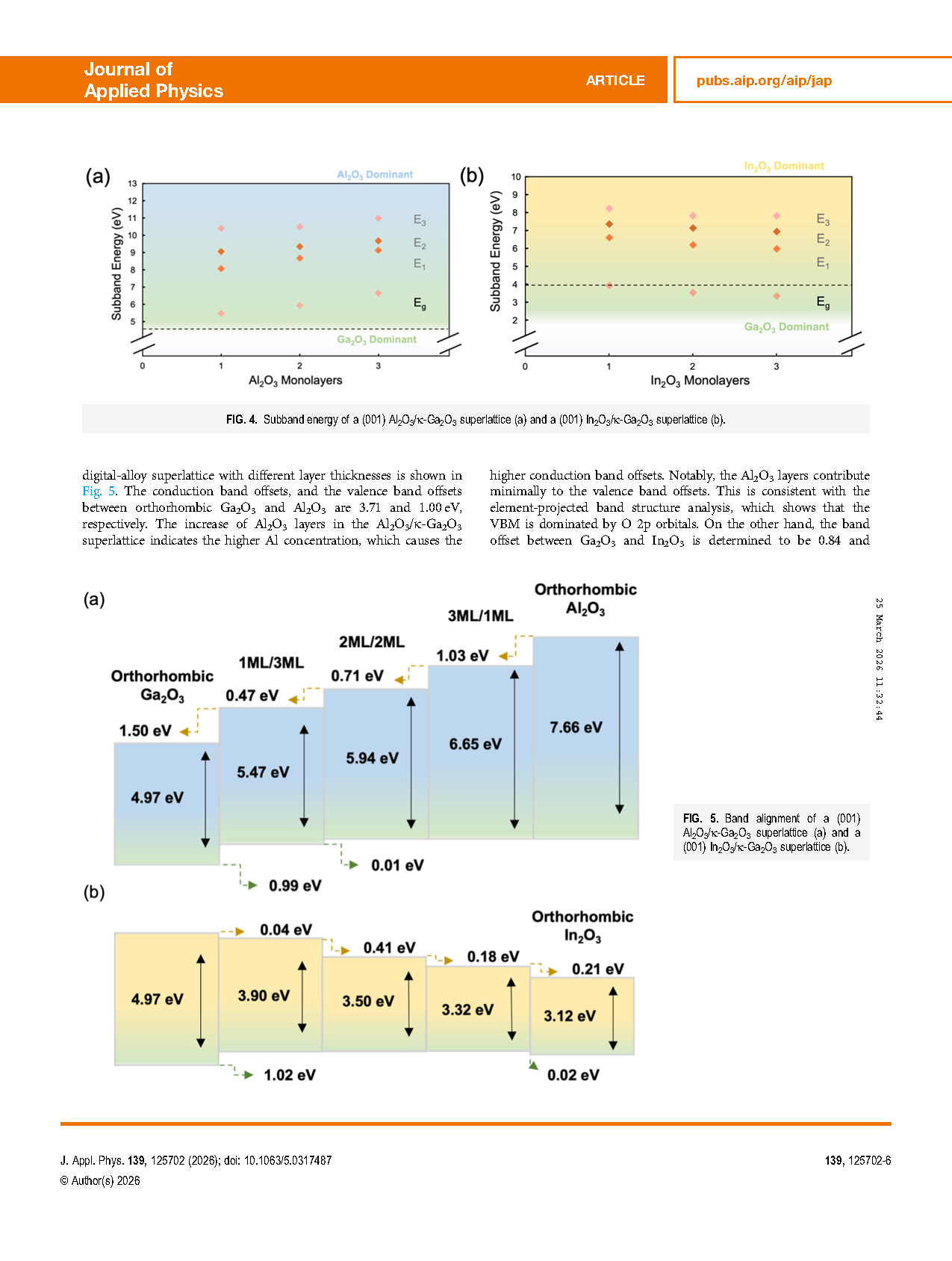
FIG. 4. Subband energy of a (001) Al2O3/κ-Ga2O3 superlattice (a) and a (001) In2O3/κ-Ga2O3 superlattice (b).
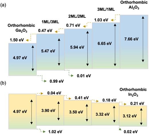
FIG. 5. Band alignment of a (001) Al2O3/κ-Ga2O3 superlattice (a) and a (001) In2O3/κ-Ga2O3 superlattice (b).
DOI:
doi.org/10.1063/5.0317487