Paper Sharing
【Member Papers】Identifying the Predominant Leakage Channel under Low Reverse Bias for β‑Ga₂O₃ Vertical Device Epitaxy on the (010) Plane
日期:2026-04-02阅读:186
Researchers from the Dalian University of Technology have published a dissertation titled "Identifying the Predominant Leakage Channel under Low Reverse Bias for β‑Ga₂O₃ Vertical Device Epitaxy on the (010) Plane" in Crystal Growth and Design.
Background
β-gallium oxide (β-Ga2O3), characterized by an ultra-wide bandgap of 4.5 eV, a high breakdown electric field strength of 8 MV/cm, and intrinsic solar-blind ultraviolet properties, has emerged as an ideal semiconductor material for high-power electronic devices and solar-blind ultraviolet photodetectors.Among the three crystallographic planes of β-Ga2O3, the epitaxial layer on the (010) substrate demonstrates a notably high electron mobility approaching the theoretical limit of approximately 200 cm² V⁻¹ s⁻¹, superior growth rates, and enhanced thermal conductivity relative to the other planes, establishing the optimal substrate plane for the growth of thick epitaxial film and the fabrication of high-performance devices. However, a large number of micron-scale hillock defects were observed on the (010) epilayer, with a density ranging from 103 to 104 cm-2, resulting in a roughened surface regardless of different growth methods. Recently, while some research has made initial investigations into the origin, features, and control methods of hillock defects, the precise effect of various types of hillock defects on device leakage behavior under low reverse bias conditions is still not well understood. Hence, the identification of the primary leakage channel in β-Ga2O3 (010) epitaxial surface vertical devices under low bias conditions, along with an understanding of their leakage mechanisms, holds considerable scientific significance and practical relevance for the advancement of high-performance β-Ga2O3 epitaxial growth and power device applications.
Abstract
In this work, the β-Ga2O3 homoepitaxial film was grown by the OVPE method on the Sn-doped β-Ga2O3 (010) substrate. Type I hillocks exhibit a rectangular shape elongated along the [001] direction, while type II hillocks are square-shaped, extending simultaneously along the [001] and [101] directions. Based on this foundation, a correlation analysis was conducted between the microstructural characteristics of two distinct types of hillock defects and their leakage behavior under low reverse bias conditions, revealing that the quantity of leakage pixels associated with type II hillocks is tens of times higher than that of type I hillocks, while the intensity of leakage current for type II hillocks is over 5 nA compared with the picoampere level for type I hillocks. This leakage phenomenon is attributed to the observation of continuous dislocation slipping in a certain direction with interconnected void-like defects inside beneath the type II hillock. At the same time, one can observe characteristic structures associated with the nanopipes that extend to the substrate surface and generate screw dislocations below. The as-fabricated Schottky barrier diode (SBD) devices, through the isolation of defect-free areas, ultimately demonstrate that type II hillocks induce several orders of magnitude higher leakage current than those of type I, identifying type II hillocks as the predominant leakage channel for (010) β-Ga2O3 vertical devices under low reverse bias conditions.
Highlights
First ever, two types of hillock defects on the β-Ga₂O₃ (010) surface are clearly distinguished, systematically defining their morphological and orientational characteristics: Type I is a rectangular structure extending along the [001] direction, and Type II is a square structure extending simultaneously along the [001] and [101] directions.
The microscopic mechanisms underlying the differences in leakage currents between two types of defects have been revealed. The study found that continuous dislocation slipping occurred in a certain direction, with interconnected void-like defects located beneath the type II hillock. At the same time, one can observe characteristic structures associated with the nanopipes that extend to the substrate surface and generate screw dislocations below. These microscopic defects collectively form effective leakage channels under low reverse bias, fundamentally explaining the root cause of the high leakage current caused by Type II hillock defects from a mechanistic perspective.
Using conductive atomic force microscopy for micro-area measurement combined with macroscopic verification of defect-isolated vertical devices, it is confirmed that type II hillock defects are the predominant leakage channel in the (010) plane β-Ga₂O₃ vertical devices under low reverse bias.
Conclusion
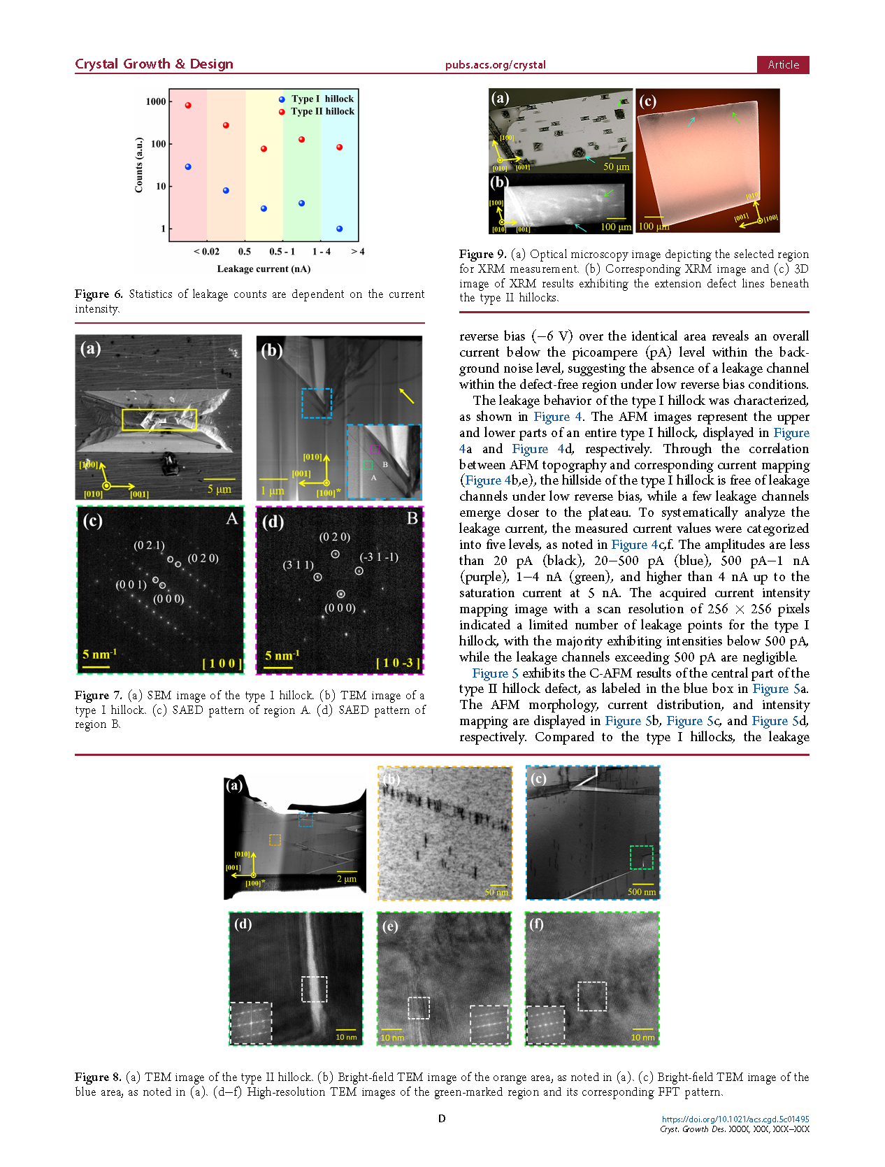
In this work, the β-Ga2O3 homoepitaxial film was grown by the OVPE method on β-Ga2O3 (010) substrate. Type I hillocks exhibit a rectangular shape elongated along the [001] direction, while type II hillocks are square-shaped, extending simultaneously along the [001] and [101] directions. Under low reverse bias, type I hillocks show results, while type II hillocks exhibit greater leakage in both intensity and quantity. This leakage phenomenon is attributed to the observation of continuous dislocation slipping in a certain direction, with interconnected void-like defects located beneath the type II hillock. At the same time, one can observe characteristic structures associated with the nanopipes that extend to the substrate surface and generate screw dislocations below. The as-fabricated SBD devices, through the isolation of defect-free areas, ultimately demonstrate that type II hillocks induce several orders of magnitude higher leakage current than those of type I, identifying type II hillocks as the major leakage channel for (010) β-Ga2O3 vertical devices under low reverse bias conditions. This study clarifies the leakage characteristics and leakage mechanisms of such devices under low reverse bias, providing important experimental evidence and ideas for defect control and performance optimization of β-Ga₂O₃ devices.
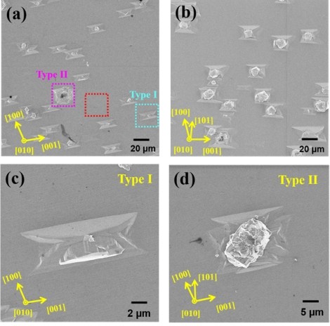
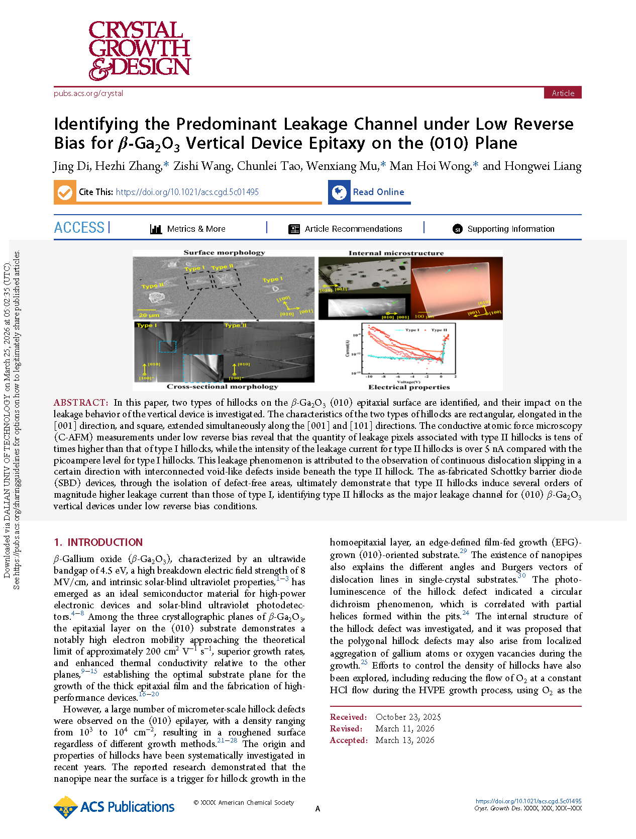
Figure 1. SEM images of the (010) surface: (a) type I hillock is predominant, (b) type II shows a wide distribution. The enlarged SEM of type I and type II hillocks, respectively, in (c) and (d).
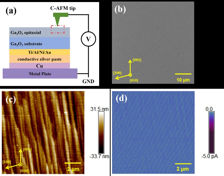
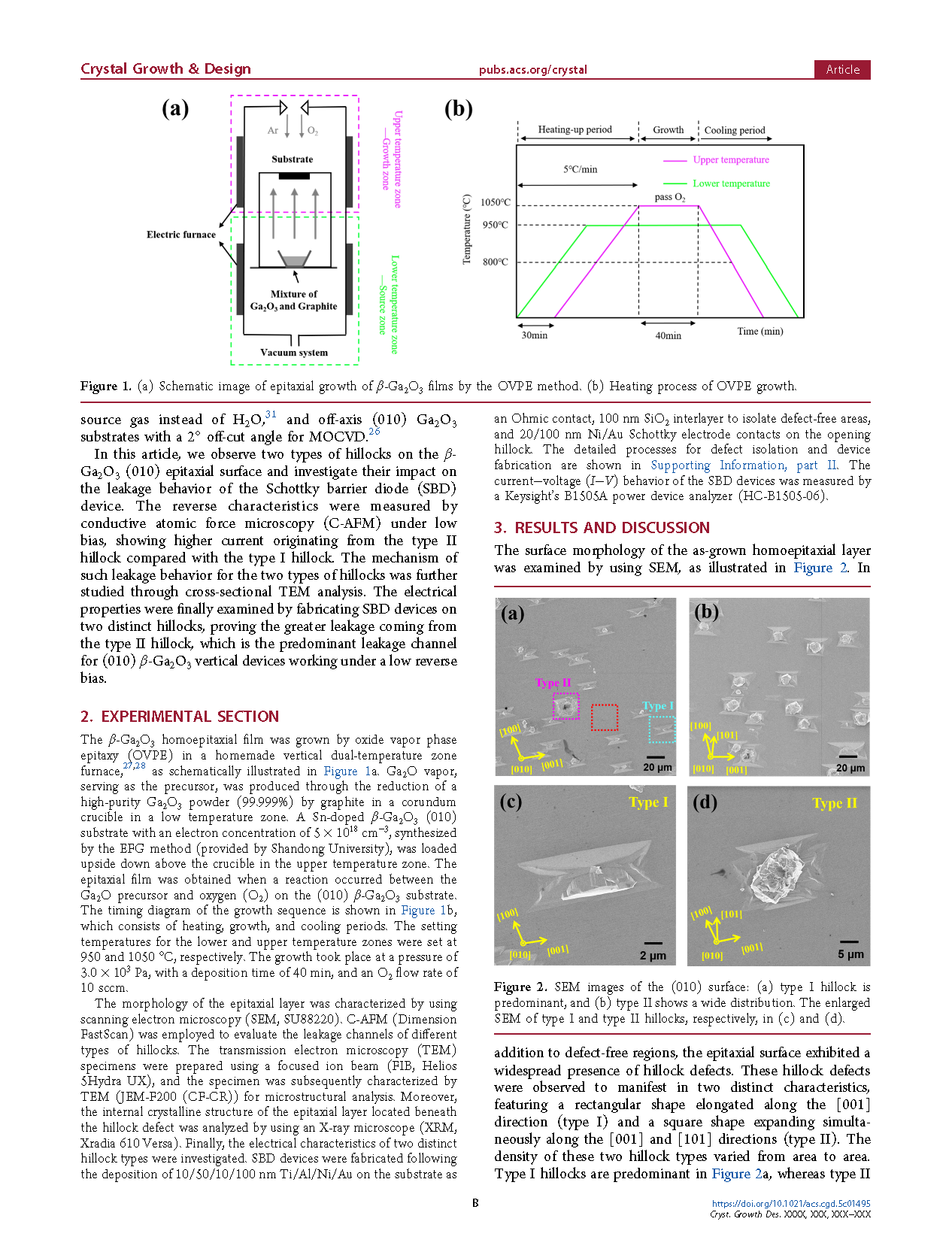
Figure 2. (a) Schematic image of C-AFM measurement setup. (b) SEM images of the defect-free area. (c) 10 × 10 µm2 AFM image of defect-free area, and (d) corresponding current mapping result measured at -6 V.
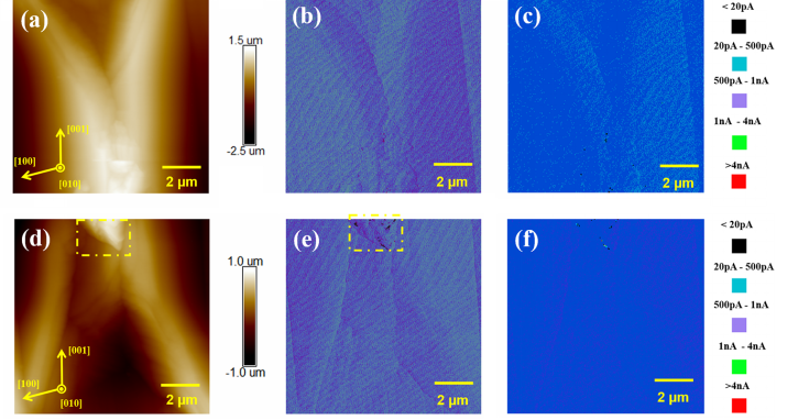
Figure 3. C-AFM images of a type I hillock. The upper part of a type I hillock: (a) AFM morphology image, (b) current mapping image measured at -6 V, (c) corresponding current intensity image. The lower part of a type I hillock: (d) AFM morphology image, (e) current mapping image measured at -6 V, (f) corresponding current intensity image.
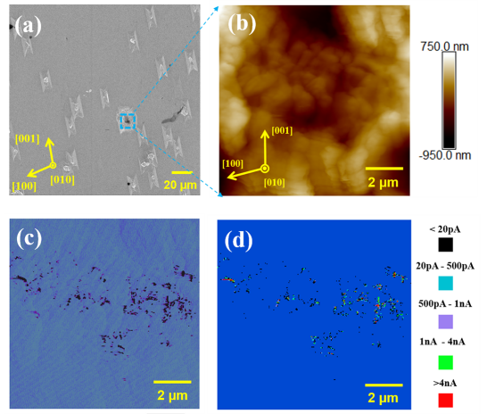
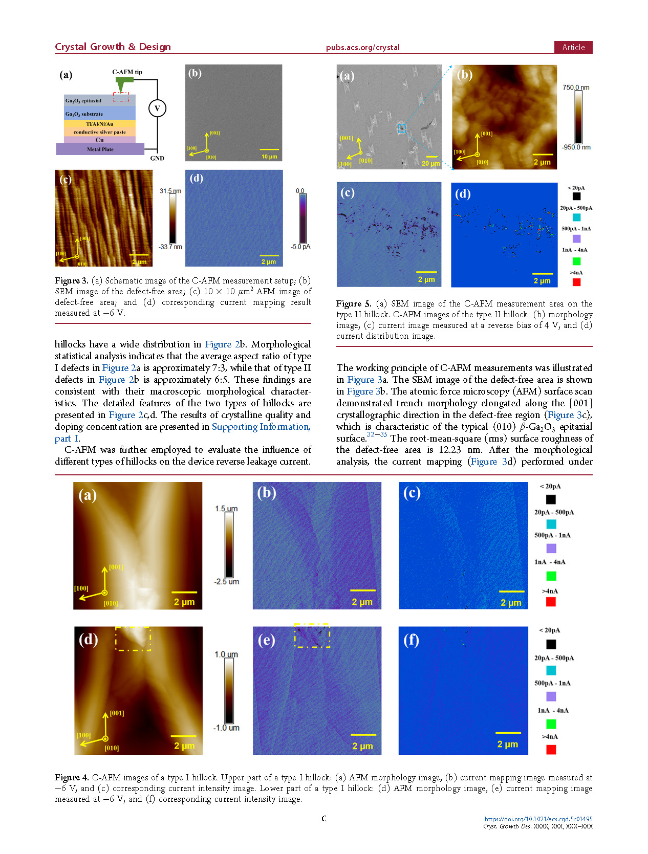
Figure 4. (a) SEM images of the C-AFM measurement area on the type II hillock. C-AFM images of the type II hillock: (b) morphology image, (c) current image measured at a reverse bias of 4 V, (d) current distribution image.
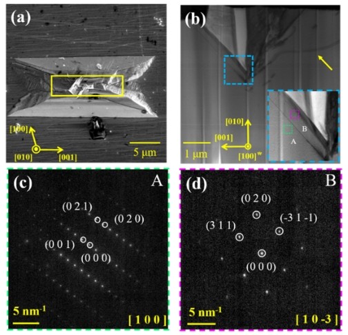
Figure 5. (a) SEM images of the type I hillock. (b) TEM images of a type I hillock. (c) The SAED pattern of region A. (d) The SAED pattern of region B.
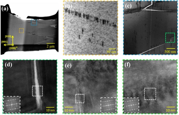
Figure 6. (a) TEM images of the type II hillock. (b) Bright-field TEM images of the orange area, as noted in Figure 8a. (c) Bright-field TEM images of the blue area, as noted in Figure 8a. (d), (e) and (f) high-resolution TEM of the green-marked region and its corresponding FFT pattern.
Figure 7. (a) The optical microscope image depicting the selected region for XRM measurement. (b) the corresponding XRM image and (c) 3D images of XRM results exhibiting the extension defect lines beneath the type II hillocks.
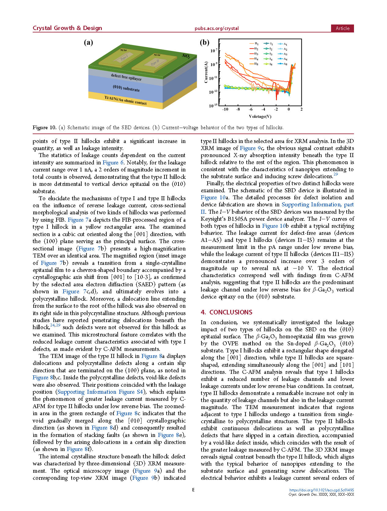
Figure 8. (a) The schematic image of the SBD devices. (b) The current-voltage behavior of the two types of hillocks.
DOI:
doi.org/10.1021/acs.cgd.5c01495