


Member News
【Member News】Breakthrough 9,000 V! Fujia Gallium Epitaxy Enables Record Ga₂O₃ MOSFET Breakdown, Ushering Power Devices into the “10 kV Era”
日期:2026-04-01阅读:342
9,000 V! This marks a major breakthrough that propels Ga₂O₃ power devices into the “10 kV era.”
On March 31, 2026, Jiufengshan Laboratory announced an exciting achievement: its team successfully developed a lateral Ga₂O₃ MOSFET with a breakdown voltage exceeding 9,000 V (measured at 9.02 kV). At a time when most reported results remain below 4,000 V, this “doubling” leap has set a new world record for Ga₂O₃ breakdown voltage, signaling that China has entered the international advanced tier in ultra-high-voltage Ga₂O₃ power device technology.
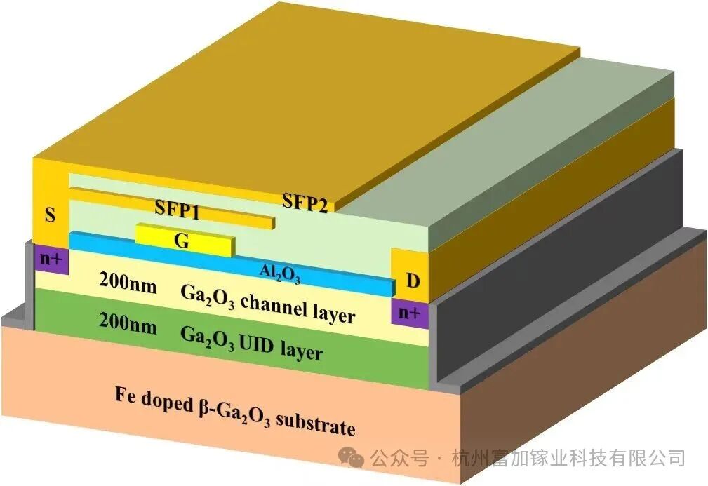
As a fellow participant in the fourth-generation semiconductor landscape—and the provider of the core material, Ga₂O₃ homoepitaxial wafers, used in this MOSFET—Fujia Gallium extends its warmest congratulations to Jiufengshan Laboratory.
Fundamental Enablement: The Strength Behind a “Domestically Produced Homoepitaxial Wafer”
In Jiufengshan Laboratory’s official announcement, one of the key factors behind this historic breakthrough was the use of a “domestically produced homoepitaxial wafer.” This wafer is a high-quality Ga₂O₃ homoepitaxial material independently developed and manufactured by Fujia Gallium.
“Great devices rely on great materials.” The crystal quality, defect density, and doping control of Ga₂O₃ epitaxial layers directly determine the performance ceiling of power devices. The leap from the industry norm of below 4,000 V to over 9,000 V not only highlights Jiufengshan Laboratory’s outstanding device design capabilities, but also underscores the critical foundational role of high-quality materials.
This is not the first time Fujia Gallium’s epitaxial wafers have received top-tier validation. Previously, vertical Schottky barrier diodes fabricated on Fujia’s epitaxial wafers achieved a power figure of merit (PFOM) of 3.07 GW/cm²—the highest value reported internationally at the time. This latest breakthrough beyond 9,000 V once again demonstrates the immense potential of Fujia’s epitaxial technology in ultra-high-voltage power electronics.
Win-Win Collaboration: Becoming the Industry’s Most Reliable “Foundation”
From achieving 8-inch breakthroughs in December 2025 to the world’s first successful development of 12-inch Ga₂O₃ single crystals in March 2026, Fujia Gallium has consistently led the scale-up revolution of fourth-generation semiconductor materials.
As one of the first companies in China to realize vertically integrated capabilities across “large-size, high-quality substrates + high-performance epitaxy (MOCVD/MBE) + device design and validation,” Fujia Gallium enables rapid internal synergy and closed-loop iteration from substrate to epitaxy to devices. This ensures superior material consistency and cost advantages for downstream partners.
“One flower does not make spring; a hundred flowers in bloom bring a full spring.” Jiufengshan Laboratory’s major breakthrough at the device level reflects the growing momentum of China’s Ga₂O₃ industry across the entire value chain—from materials to applications.
Fujia Gallium remains committed to open collaboration and to serving as a solid and reliable “foundation” for the industry. We warmly welcome global power device manufacturers, research institutions, and partners across the supply chain to join us in exploring the vast potential of fourth-generation semiconductors and accelerating the industrialization of this trillion-dollar market.
Product Portfolio
Gallium Oxide Crystal Growth Equipment
Fujia Gallium has developed the world’s first EFG crystal growth system featuring a proprietary “one-click crystal growth” function, supporting 2-inch to 6-inch crystal production. The system is protected by 6 granted domestic patents and 4 international patents. Complete equipment solutions and process packages are available.
The company has also independently developed fully automated VB (Vertical Bridgman) crystal growth equipment. It was the first in China to overcome the technical bottleneck of 6-inch single-crystal growth using the VB method, enabling large-diameter bulk crystal production. This platform is supported by 6 granted domestic patents and 4 international patents, with customizable equipment and process solutions available.
Gallium Oxide Single-Crystal Substrates
As one of China’s earliest pioneers in Gallium Oxide single-crystal research and an industry-leading supplier, Fujia Gallium provides high-quality single-crystal substrates to global customers.
The product portfolio includes 26 standard substrate specifications ranging from 2-inch to 6-inch diameters. Customized solutions are available in terms of wafer size, electrical properties, and crystal orientation, supporting both advanced epitaxy R&D and volume production requirements.
Gallium Oxide Epitaxial Wafers
Built upon mature MOCVD (Metal-Organic Chemical Vapor Deposition) and MBE (Molecular Beam Epitaxy) platforms, Fujia Gallium offers 15 standard epitaxial wafer products from 2-inch to 6-inch formats, as well as customized MBE-based epitaxial structures.
The company provides integrated “substrate + epitaxy” solutions. A precise process control system enables customization of key parameters including epitaxial layer thickness, doping concentration, and compositional uniformity, meeting diverse requirements across different power levels and device architectures.
About Hangzhou Fujia Gallium
Hangzhou Fujia Gallium Technology Co., Ltd., established on December 31, 2019, is committed to the vision of “enabling the world with better materials” and focuses on the industrialization of ultra-wide bandgap Gallium Oxide semiconductor materials. Its core products include Gallium Oxide single-crystal substrates, MOCVD/MBE epitaxial wafers, and crystal growth equipment based on the Vertical Bridgman (VB) and Edge-Defined Film-Fed Growth (EFG) methods. The company provides systematic solutions for material development, accelerating the integration of the entire ultra-wide bandgap Gallium Oxide industry chain and promoting the application of Gallium Oxide materials in power devices, microwave RF devices, and optoelectronic detection. A series of major achievements in Gallium Oxide development have been featured by leading media outlets including CCTV-1, CCTV-2, People’s Daily, Xinhua News Agency, China Securities Journal, and The Paper.
In terms of corporate recognition, the company was designated as a Zhejiang Province Science and Technology SME in 2022, recognized as a National High-Tech Enterprise in 2023, and awarded the titles of Hangzhou High-Tech Enterprise R&D Center and Zhejiang “Specialized and Sophisticated” SME in 2024. In 2025, it obtained ISO 9001 Quality Management System certification (Certificate No. 20225Q20294R0M) and was also named a 2024 Hangzhou “New Eagle” Enterprise. In the Gallium Oxide field, the company is leading the drafting of the first national standard in this area and has undertaken one project from the National Development and Reform Commission and one from the Ministry of Industry and Information Technology, while participating in three additional national and provincial-level projects supported by the National Natural Science Foundation of China and regional authorities in Zhejiang and Shanghai. To date, the company has been granted 14 international patents (6 in the United States, 7 in Japan, and 1 in Europe), 42 domestic patents, three registered “Fujia Gallium” trademarks, and five software copyrights, including its proprietary “One-Click Crystal Growth” control software.
