Paper Sharing
【Domestic Papers】Achieving programmable bipolar photocurrents via p–n junction design for PEPS-based optoelectronic applications
日期:2026-04-01阅读:158
Researchers from Zhejiang Sci-Tech University have published a dissertation titled " Achieving programmable bipolar photocurrents via p–n junction design for PEPS-based optoelectronic applications " in Applied Physics Letters.
Background
The photoelectrochemical photocurrent switching (PEPS) effect, where a single photodetector generates photocurrent responses of opposite polarities under varied conditions, is a remarkable phenome non that has garnered significant attention in the fields of optoelec tronic functional materials and devices in recent years.This effect not only provides a crucial perspective for understanding the separa tion, transport, and collection mechanisms of photogenerated carriers at heterojunctions but also shows great potential in frontier applica tions such as photoelectric logic operations,5,6 optical communica tion,and self-powered sensing.The ability to precisely control the direction and magnitude of the photocurrent thus enables advanced signal manipulation, laying the groundwork for the develop ment of a newgeneration of intelligent optoelectronic systems.
Abstract
The photoelectrochemical photocurrent switching (PEPS) effect, which enables a single photodetector to generate opposite photocurrent polarities under varied conditions, offers key insights into carrier dynamics at heterojunctions and holds promise for advanced applications in photoelectric logic, optical communication, and self-powered sensing. To achieve wavelength-programmable bipolar photocurrents, this study designed two distinct heterojunctions, such as a p–n junction (Cu2O/a-Ga2O3) and an n–n junction (CdS/a-Ga2O3), and compared their PEPS behaviors. The designed p–n junction successfully realized the desired PEPS effect at 0V bias, exhibiting a positive photocurrent under 254nm UV light and a negative photocurrent under 365nm illumination. In contrast, the n–n junction showed no such polarity switching. This functional difference is attributed to the strong, unidirectional built-in electric field engineered into the p–n junction, which orchestrates wavelength-selective carrier transport and thus dictates the photocurrent polarity. The weaker, diffuse field in the n–n junction fails to achieve this directional control. By leveraging the programmable bipolar photoresponse of the designed p–n device, we further demon strated its application as a single-element half-adder for simplified logic circuits and its potential for high-density coding and binary phase shift keying modulation in optical communication. This work confirms that intentional band engineering through heterojunction design is the key to materializing the PEPS effect, providing a clear design principle and material platform for developing advanced intelligent photo electrochemical devices.
Conclusion
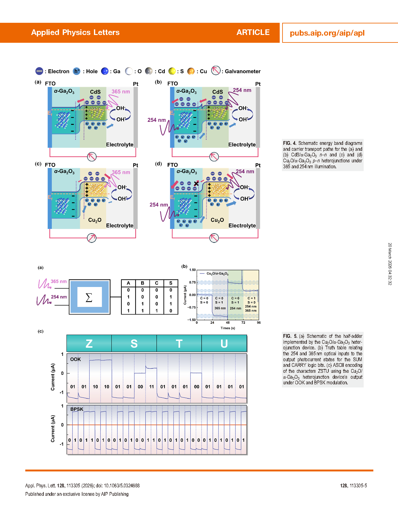
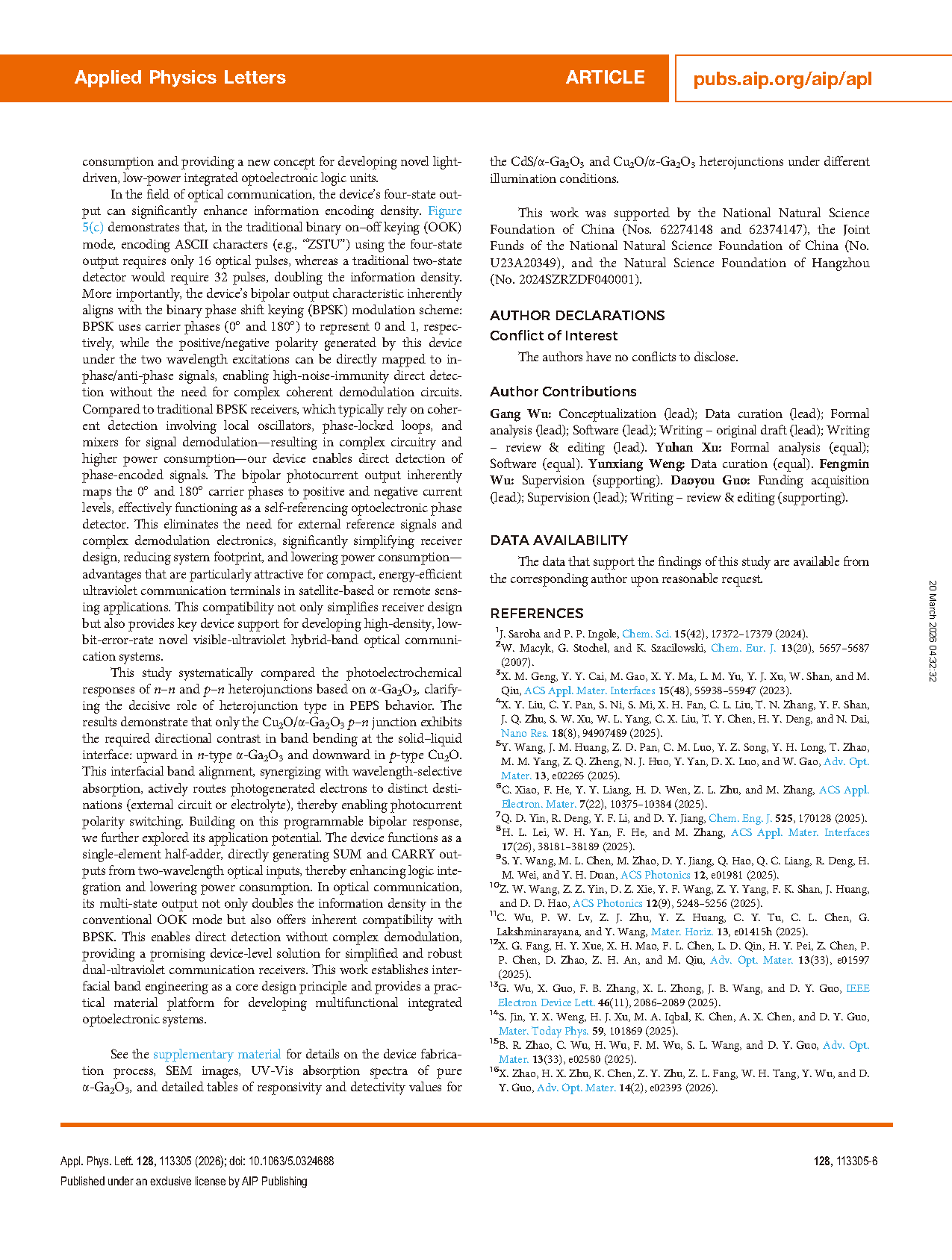
This study systematically compared the photoelectrochemical responses of n–n and p–n heterojunctions based on a-Ga2O3,clarify ing the decisive role of heterojunction type in PEPS behavior. The results demonstrate that only the Cu2O/a-Ga2O3 p–n junction exhibits the required directional contrast in band bending at the solid–liquid interface: upward in n-type a-Ga2O3 and downward in p-type Cu2O. This interfacial band alignment, synergizing with wavelength-selective absorption, actively routes photogenerated electrons to distinct desti nations (external circuit or electrolyte), thereby enabling photocurrent polarity switching. Building on this programmable bipolar response, we further explored its application potential. The device functions as a single-element half-adder, directly generating SUM and CARRY out puts from two-wavelength optical inputs, thereby enhancing logic inte gration and lowering power consumption. In optical communication, its multi-state output not only doubles the information density in the conventional OOK mode but also offers inherent compatibility with BPSK. This enables direct detection without complex demodulation, providing a promising device-level solution for simplified and robust dual-ultraviolet communication receivers. This work establishes inter facial band engineering as a core design principle and provides a prac tical material platform for developing multifunctional integrated optoelectronic systems.
Project Support
This work was supported by the National Natural Science Foundation of China (Nos. 62274148 and 62374147), the Joint Funds of the National Natural Science Foundation of China (No. U23A20349), and the Natural Science Foundation of Hangzhou (No. 2024SZRZDF040001).
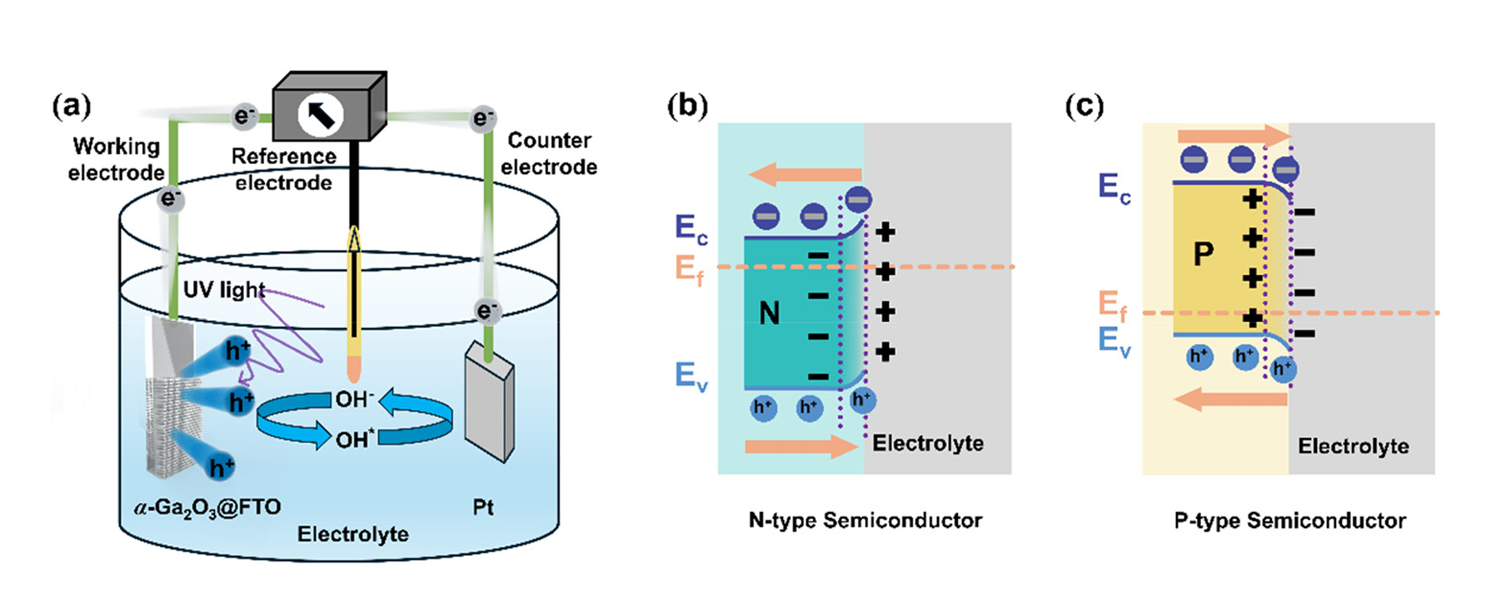
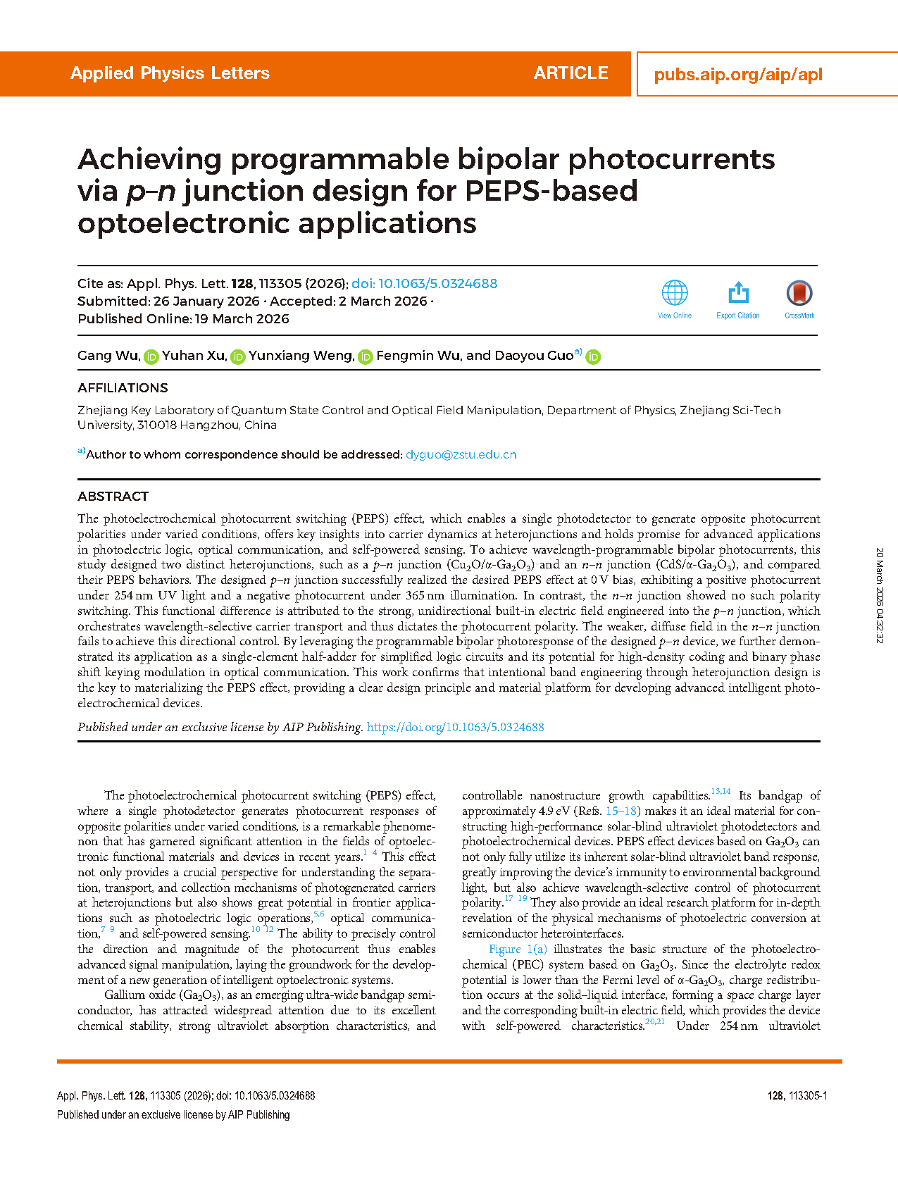
FIG. 1. (a) Schematic illustration of the PEC system based on a Ga₂O₃ photoanode. Energy band diagrams comparing the charge carrier dynamics in PEC systems employing (b) n-type and (c) p-type semiconductors.
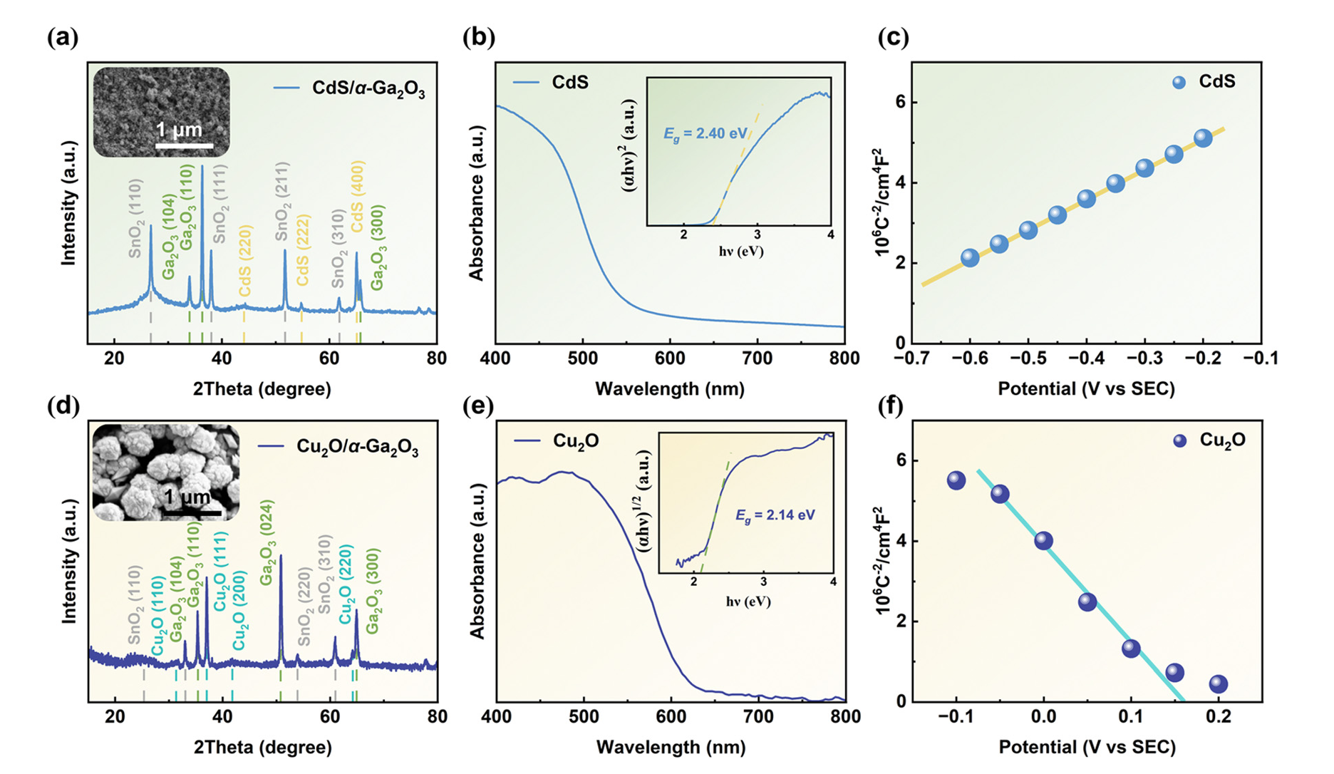
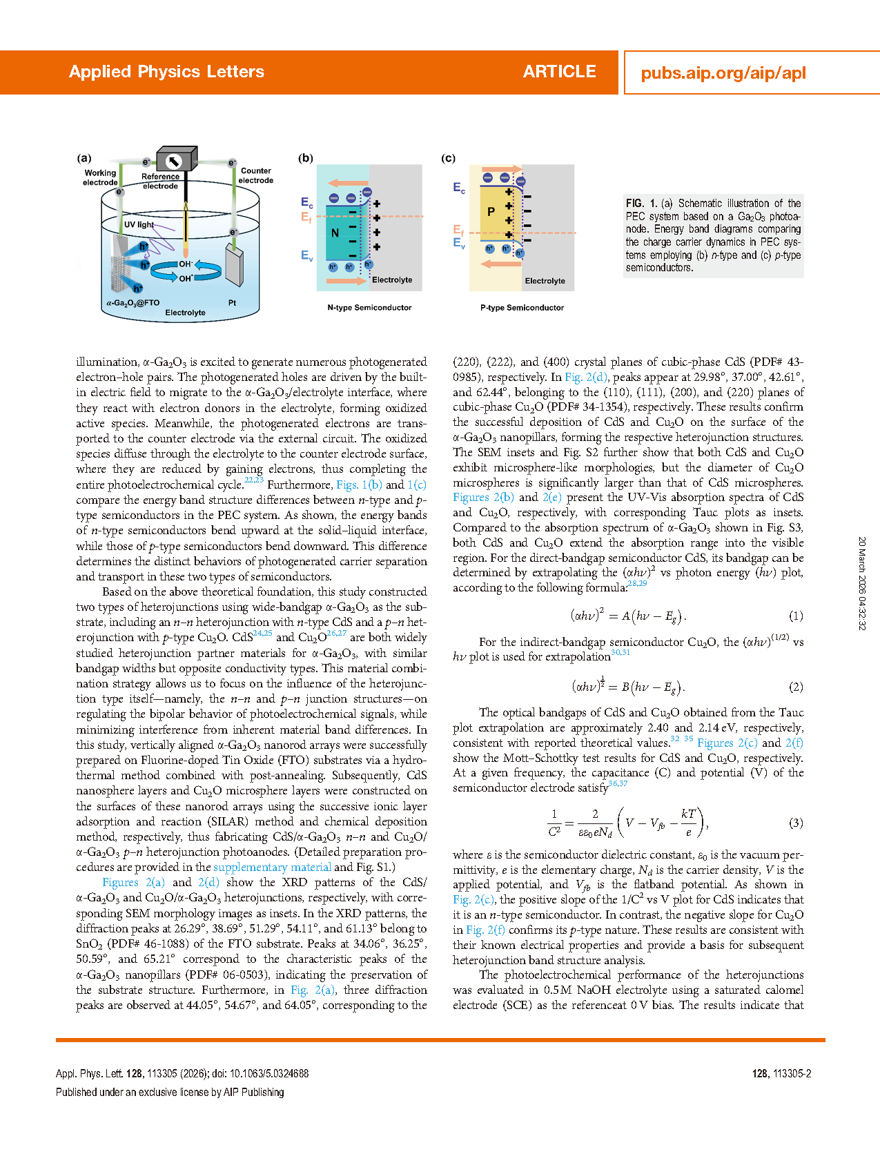
FIG. 2. (a) XRD pattern of the CdS/a-Ga₂O₃ n–n heterojunction, with a corresponding SEM image in the inset.(b) UV-Vis absorption spectrum of CdS, with the Tauc plot for bandgap determination in the inset.(c) Mott–Schottky plot of the CdS film.(d)–(f) Corresponding characterization results (XRD with SEM inset, absorption spectrum with Tauc plot inset, and Mott–Schottky plot) for the Cu₂O/a-Ga₂O₃ p–n heterojunction.
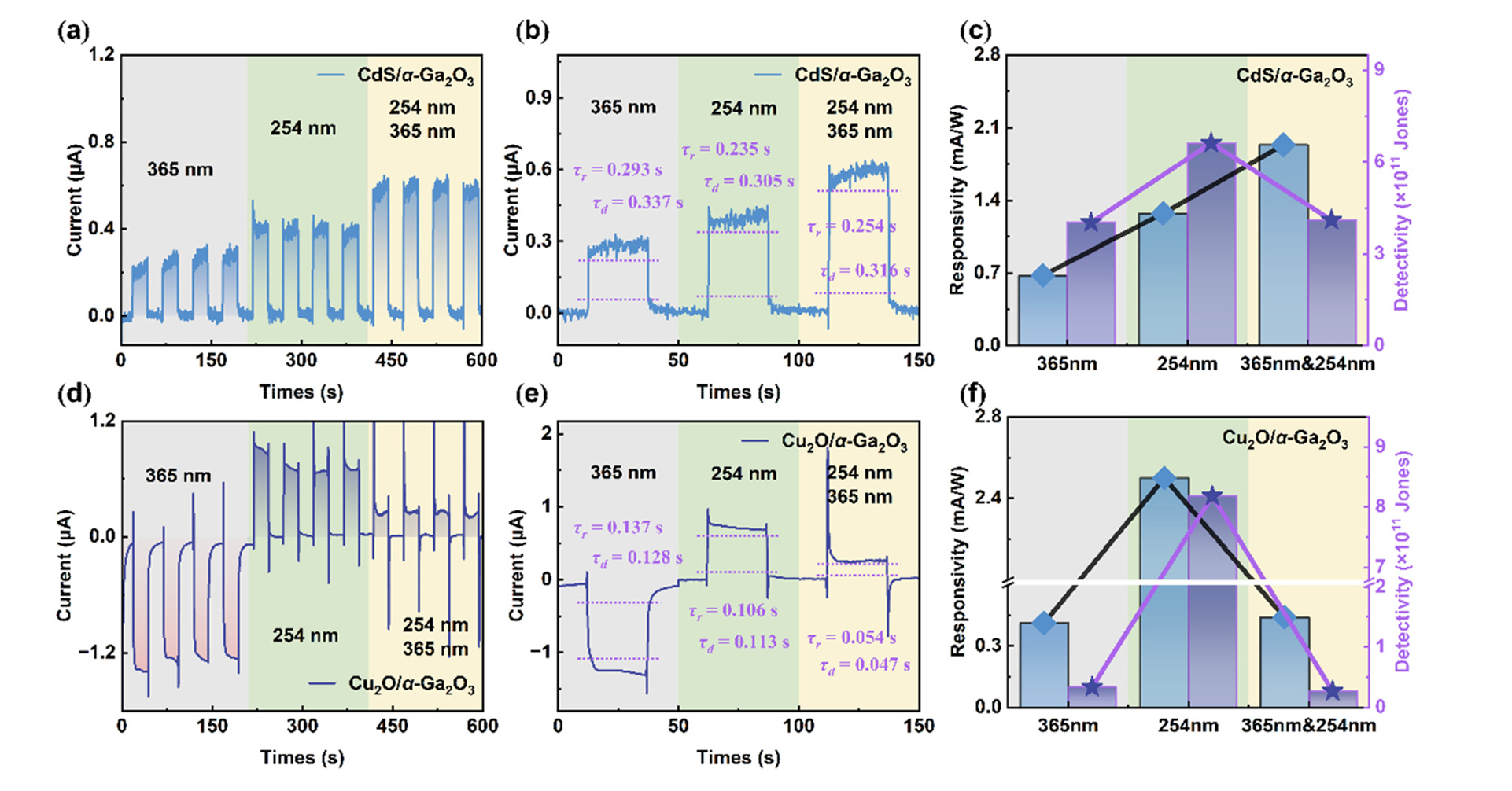
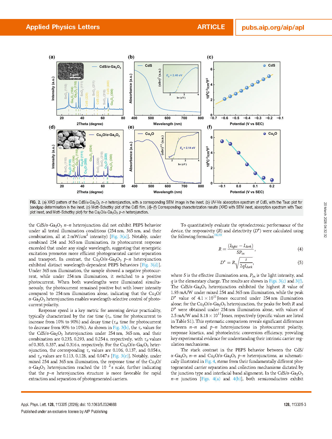
FIG. 3. (a) Photocurrent response of the CdS/a-Ga₂O₃ n–n heterojunction under 254 nm, 365 nm, and combined illumination at 0 V.(b) Corresponding response time (τᵣ) and decay time (τd) analysis.(c) Calculated responsivity and detectivity under different illumination conditions for the n–n junction.(d)–(f) Parallel set of results (photocurrent response, response times, and figures of responsivity and detectivity) for the Cu₂O/a-Ga₂O₃ p–n heterojunction.
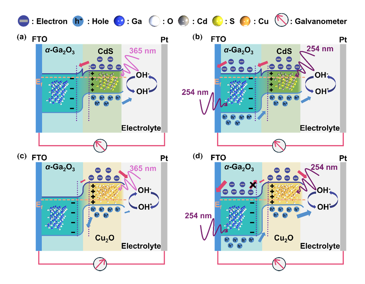
FIG. 4. Schematic energy band diagrams and carrier transport paths for the (a) and (b) CdS/a-Ga2O3 n–n and (c) and (d) Cu2O/a-Ga2O3 p–n heterojunctions under 365 and 254nm illumination.
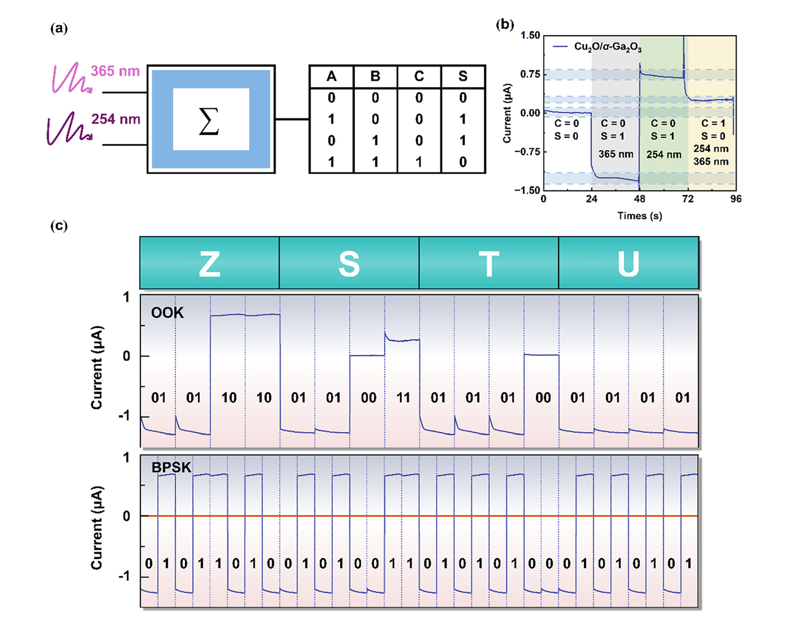
FIG. 5. (a) Schematic of the half-adder implemented by the Cu2O/a-Ga2O3 heter ojunction device. (b) Truth table relating the 254 and 365nm optical inputs to the output photocurrent states for the SUM and CARRY logic bits. (c) ASCII encoding of the characters ZSTU using the Cu2O/ a-Ga2O3 heterojunction device’s output under OOK and BPSK modulation.
DOI:
doi.org/10.1063/5.0324688