Paper Sharing
【International Papers】Self-Rectifying Dynamic Memristor Based on 2D-Graphene/V-doped Ga₂O₃ for Neuromorphic Processing
日期:2026-04-01阅读:163
Researchers from the Ajou University have published a dissertation titled "Self-Rectifying Dynamic Memristor Based on 2D-Graphene/V-doped Ga2O3 for Neuromorphic Processing" in Materials Today Physics.
Background
Traditional digital computers follow the von Neumann paradigm, which separates memory and computation and creates a data-transfer bottleneck that limits throughput and energy efficiency-especially for AI tasks that demand real-time pattern recognition, continual learning, adaptation, and massive parallelism. Neuromorphic computing based on resistive random-access memory (RRAM) has therefore become a major direction for advancing AI and reservoir computing. RRAM devices are attractive for memory, logic, neural networks, and sensing because of their simple structures, high integration density, low power operation, and fast switching, while enabling in-memory processing that minimizes data movement. In metal-oxide RRAM, electric-field-induced SET/RESET produces multi-level, history-dependent states that emulate synaptic plasticity and support networks of artificial neurons and synapses. Importantly for wearable and conformal electronics, RRAM can be fabricated on flexible substrates (e.g., polyimide) with transparent or ultrathin electrodes (graphene, Ag-nanowires, ITO), sustaining reliable switching under small bending radii and repeated flexing, which makes them well-suited for flexible, real-time neuromorphic systems.
Abstract
Memristors adjust their internal resistance in response to external stimuli, enabling random-access memory, neuromorphic computing, sensing, and in-memory processing functions that are difficult to achieve with conventional devices. These capabilities arise from diverse switching mechanisms, making mechanistic understanding and the discovery of new memristive operation modes crucial for reliable implementation and advanced applications. In this work, we present a flexible Au/V-doped a-Ga2O3/single-layer graphene (SL-Gr)/Cu memristor platform, benchmarked against a reference device without graphene, in which mechanical strain directly modulates the switching mechanism. The SL-Gr interlayer regulates Cu+ injection and diffusion so that Cu-rich nanoclusters nucleate predominantly at graphene defect and edge sites (ECM contribution), while concurrent oxygen-vacancy (Vo) enrichment and field-driven redox in the V-doped a-Ga2O3 contribute to a valence-change pathway (VCM contribution), yielding a controllable hybrid-filament system. Notably, under stable and flexible operation, the device exhibits key neuromorphic functions, including Pavlovian associative learning, image memorization in a 3 × 3 array of letter “C”, “F”, “I”, and “L”, 4-bit state encoding, and digit recognition within a reservoir computing (RC) framework, underscoring its potential as a promising candidate for next-generation artificial intelligent (AI) hardware.
Highlights
A flexible, forming-free Au/V-doped amorphous (a)-Ga2O3/SL-Graphene/Cu memristor is realized, delivering stable self-rectifying and compliance-free resistive switching.
Graphene interlayer precisely controls Cu + injection and enables a strain-tunable hybrid ECM-VCM mechanism with robust filament dynamics.
The device emulates essential neuromorphic behaviors, including symmetric LTP/LTD, PPF, STM-LTM transition, Pavlovian learning, and 3 × 3 image memorization.
A memristor-based reservoir computing system achieves deterministic multilevel states, 4-bit encoding, and accurate digit recognition for compact AI hardware.
Conclusion
In summary, we demonstrate a self-rectifying, forming-free, and stable Au/V-doped a-Ga2O3/single-layer graphene (SL-Gr)/Cu memristor that unifies reliable resistive switching, rich neuromorphic plasticity, and hardware-efficient reservoir computing within a single flexible platform. Comprehensive structural, spectroscopic, and DFT analyses confirm the formation of amorphous V-doped a-Ga2O3 with mixed-valence V4+/V5+ states and engineered defect levels, enabling controlled electronic transport and providing a rational basis for the observed device characteristics. The insertion of an atomically thin graphene interlayer between Cu and V-doped a-Ga2O3 suppresses uncontrolled Cu penetration, owing to hybrid ECM-VCM soft-filament mechanism in which Cu-rich nanoclusters and oxygen-vacancy-enriched pathways co-operatively govern conduction. This architecture delivers self-limited, compliance-free switching with a large memory window, excellent cycle-to-cycle and device-to-device uniformity, and stable operation under bending, evidencing strain-tunable yet robust filament dynamics ideally suited for flexible electronics.
Beyond memory function, the device operates as an artificial synapse capable of emulating key biological learning rules, including gradual and symmetric LTP/LTD, interval-dependent nonlinearity tuning, paired-pulse facilitation (PPF), STM-to-LTM transition, Pavlovian associative learning, and image memorization in a 3 × 3 array. These rich, tunable dynamics are further exploited in a proof-of-concept reservoir computing framework, where deterministic multilevel conductance states and transient responses enable robust 4-bit state encoding and digit recognition using a minimal array, underscoring the scalability and computational relevance of the proposed system. Collectively, our results position the 2D-single-layer graphene/V-doped Ga2O3 flexible memristor as a promising building block for next-generation flexible in-memory computing, neuromorphic systems, and compact, AI hardware.
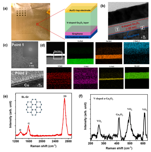
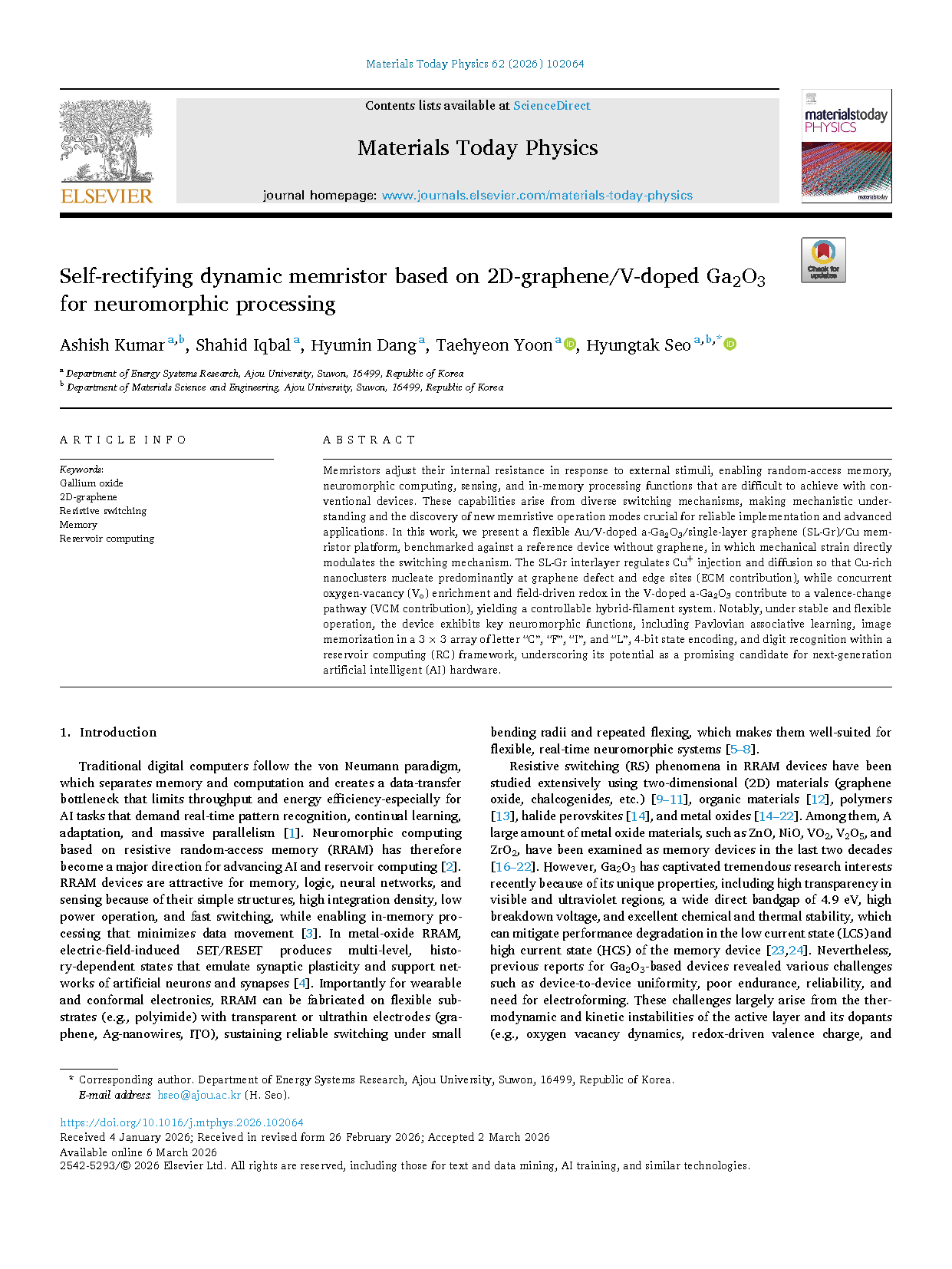
Fig. 1. (a) Schematic illustration of Au/V-doped a-Ga2O3/single-layer graphene (SL-Gr)/Cu structure. (b) Cross-sectional transmission electron microscopy (TEM) image of the device, showing the layered structure of Au, Cr, V-doped a-Ga2O3, single-layer (SL) graphene (GR), and Cu (crystalline). (c) The zoomed-in regions provide a detailed view of the interface, highlighting the crystalline quality of each layer. The Ga2O3 amorphous layer, as shown in the Fast Fourier Transform (FFT) image in the insert. SL-Gr is crystalline, exhibiting an atomic arrangement. (d) TEM-EDS mapping of the thin film with a scale bar of 100 nm. (e)-(f) Raman pattern of SL-Gr, and V-doped a-Ga2O3 measured under 532 nm excitation.
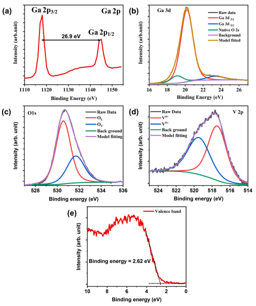
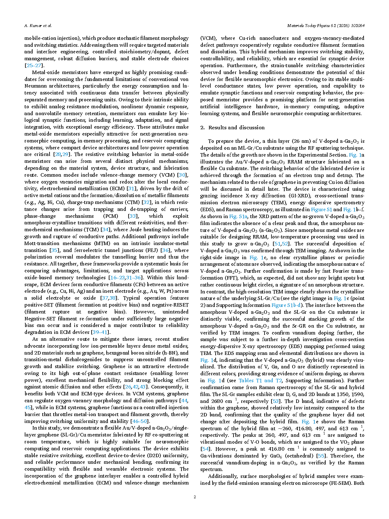
Fig. 2. X-ray photoelectron spectroscopy (XPS) of V-doped a-Ga2O3 thin film, (a) Ga 2p doublet (Ga 2p3/2 and 2p1/2) indicative of Ga3+, (b) Ga 3d- O 2s region showing Ga 3d components and O 2s band, (c) O 1s deconvolution into lattice oxygen and vacancy/OH- related species, (d) V 2p3/2 fiitted with V4+ and V5+ contribution, evidencind mixed valence, and (e) VBM at ~2.62 eV.
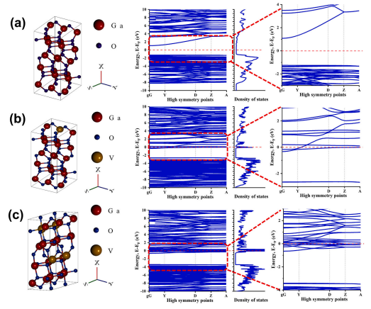
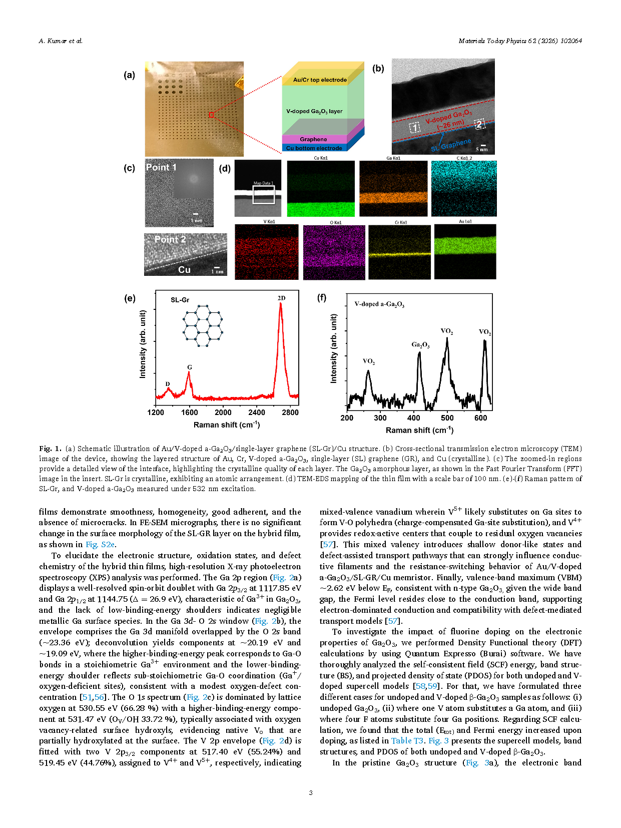
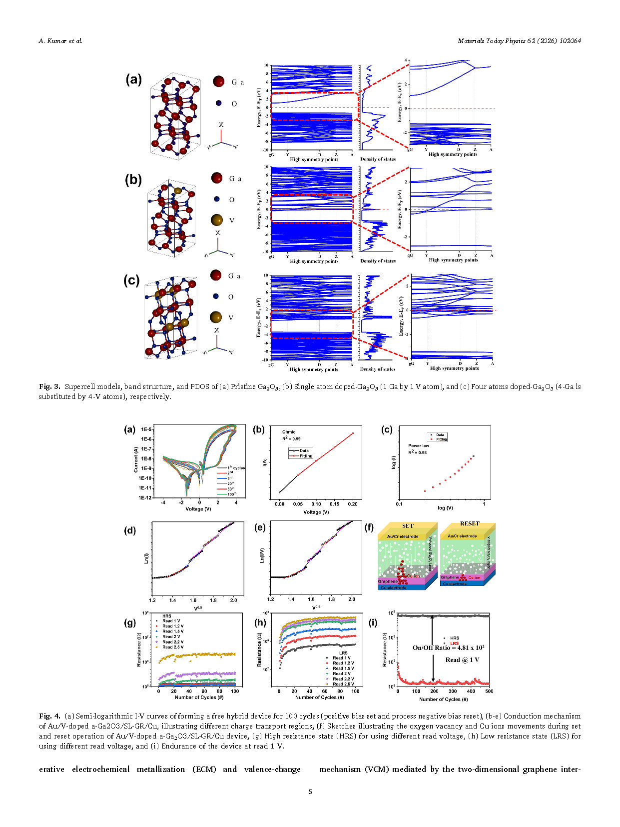
Fig. 3. Supercell models, band structure, and PDOS of (a) Pristine Ga2O3, (b) Single atom doped-Ga2O3 (1 Ga by 1 V atom), and (c) Four atoms doped-Ga2O3 (4-Ga is substituted by 4-V atoms), respectively.
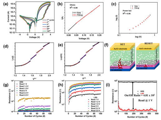
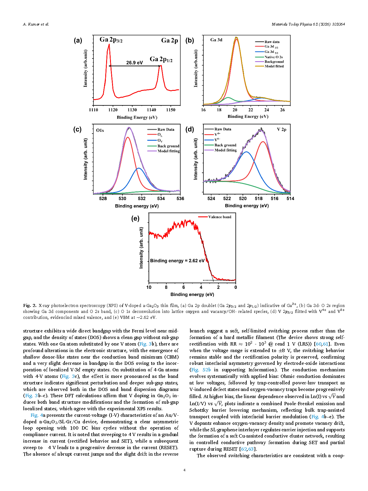
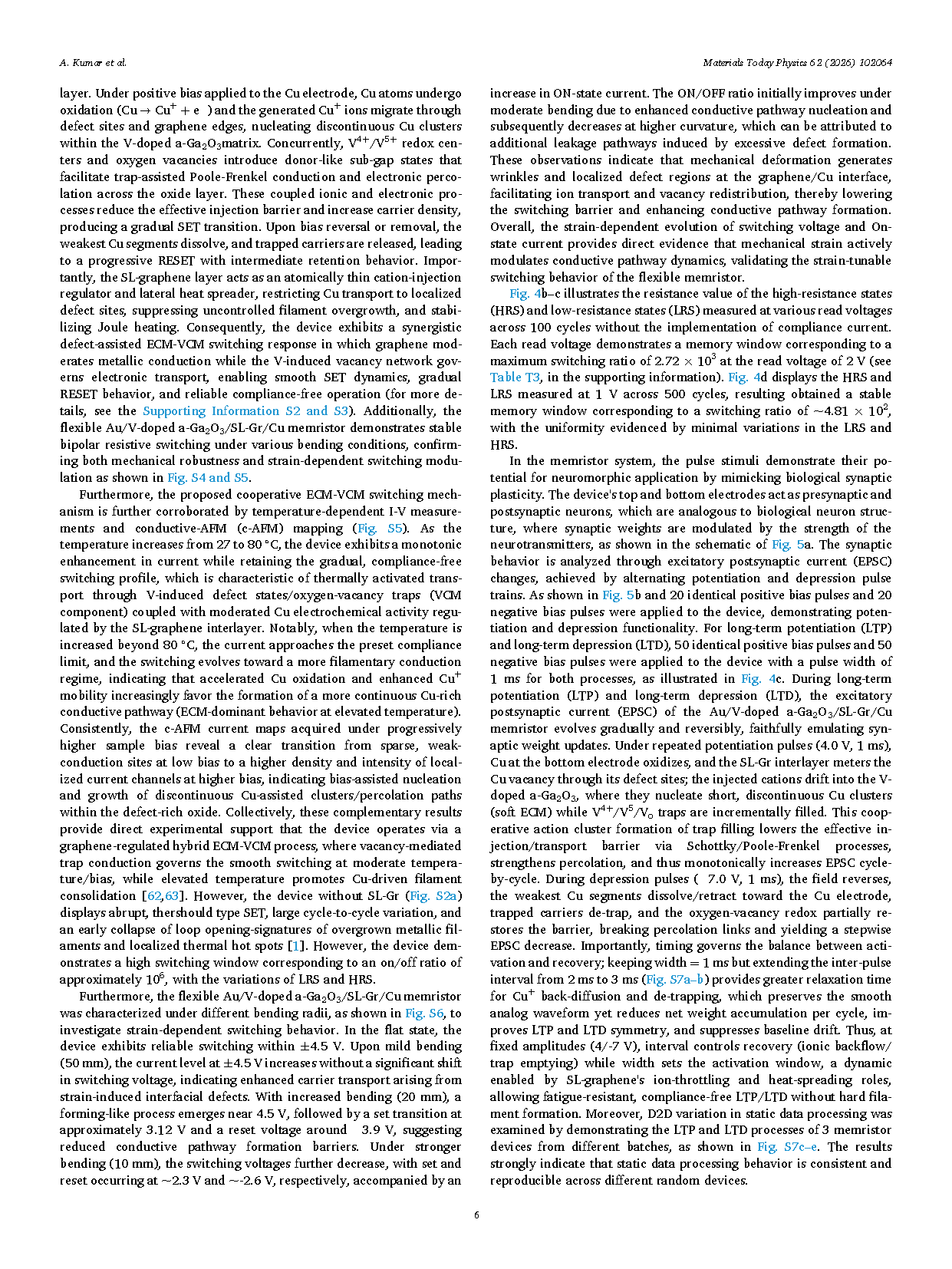
Fig. 4. (a) Semi-logarithmic I-V curves of forming a free hybrid device for 100 cycles (positive bias set and process negative bias reset), (b-e) Conduction mechanism of Au/V-doped a-Ga2O3/SL-GR/Cu, illustrating different charge transport regions, (f) Sketches illustrating the oxygen vacancy and Cu ions movements during set and reset operation of Au/V-doped a-Ga2O3/SL-GR/Cu device, (g) High resistance state (HRS) for using different read voltage, (h) Low resistance state (LRS) for using different read voltage, and (i) Endurance of the device at read 1 V.
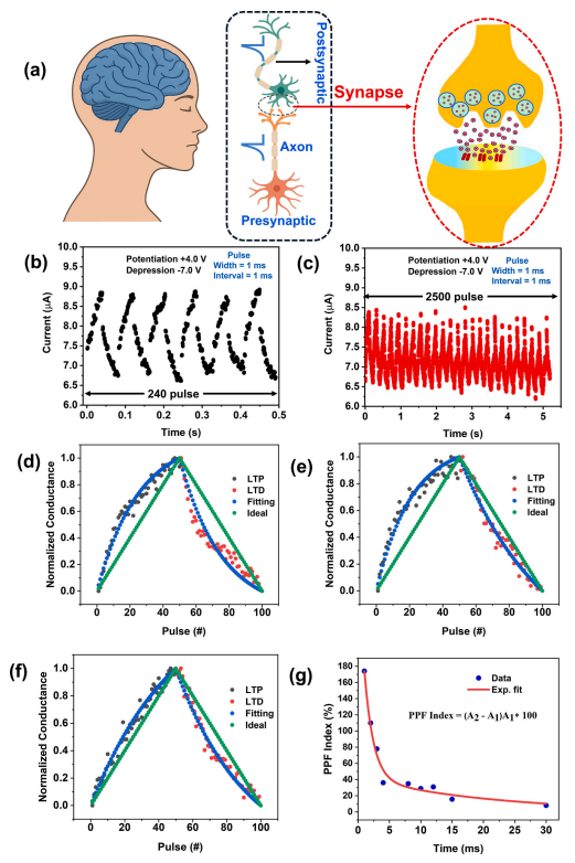
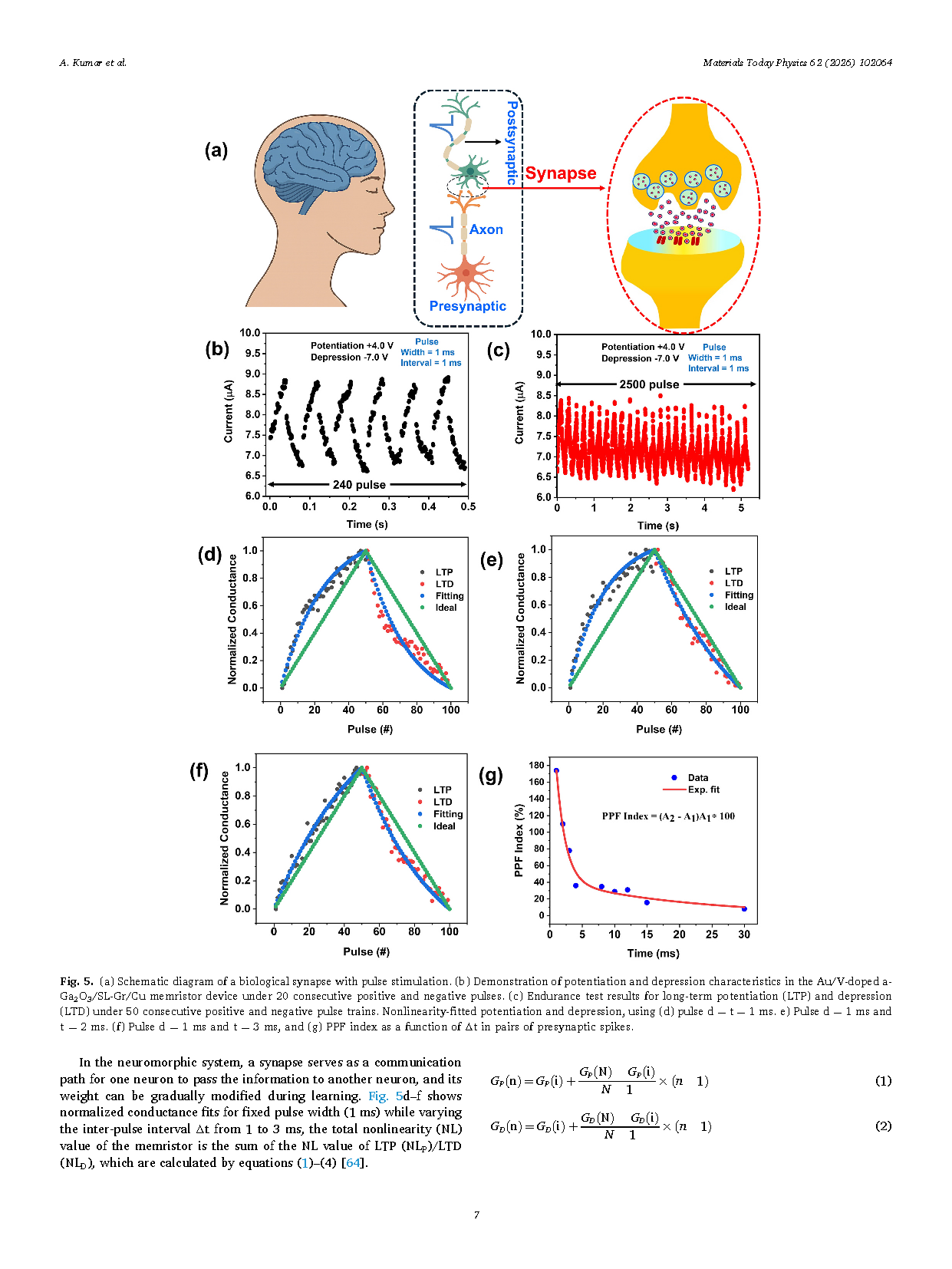
Fig. 5. (a) Schematic diagram of a biological synapse with pulse stimulation. (b) Demonstration of potentiation and depression characteristics in the Au/V-doped a-Ga2O3/SL-Gr/Cu memristor device under 20 consecutive positive and negative pulses. (c) Endurance test results for long-term potentiation (LTP) and depression (LTD) under 50 consecutive positive and negative pulse trains. Nonlinearity-fitted potentiation and depression, using (d) pulse d = t = 1 ms. e) Pulse d = 1 ms and t = 2 ms. (f) Pulse d = 1 ms and t = 3 ms, and (g) PPF index as a function of Δt in pairs of presynaptic spikes.
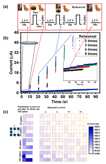
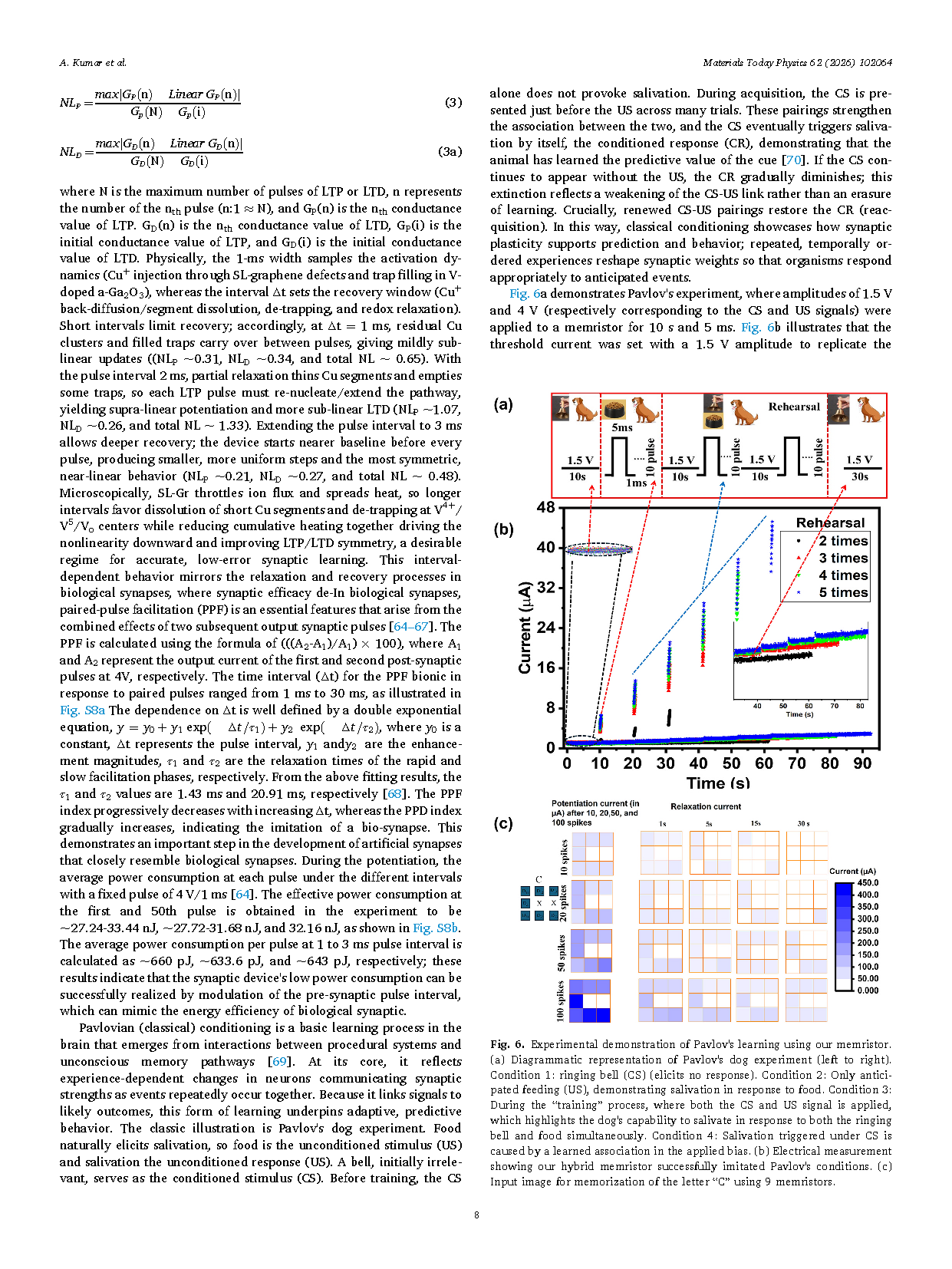
Fig. 6. Experimental demonstration of Pavlov's learning using our memristor. (a) Diagrammatic representation of Pavlov's dog experiment (left to right). Condition 1: ringing bell (CS) (elicits no response). Condition 2: Only anticipated feeding (US), demonstrating salivation in response to food. Condition 3: During the “training” process, where both the CS and US signal is applied, which highlights the dog's capability to salivate in response to both the ringing bell and food simultaneously. Condition 4: Salivation triggered under CS is caused by a learned association in the applied bias. (b) Electrical measurement showing our hybrid memristor successfully imitated Pavlov's conditions. (c) Input image for memorization of the letter “C” using 9 memristors.
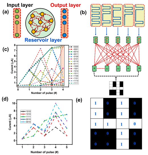
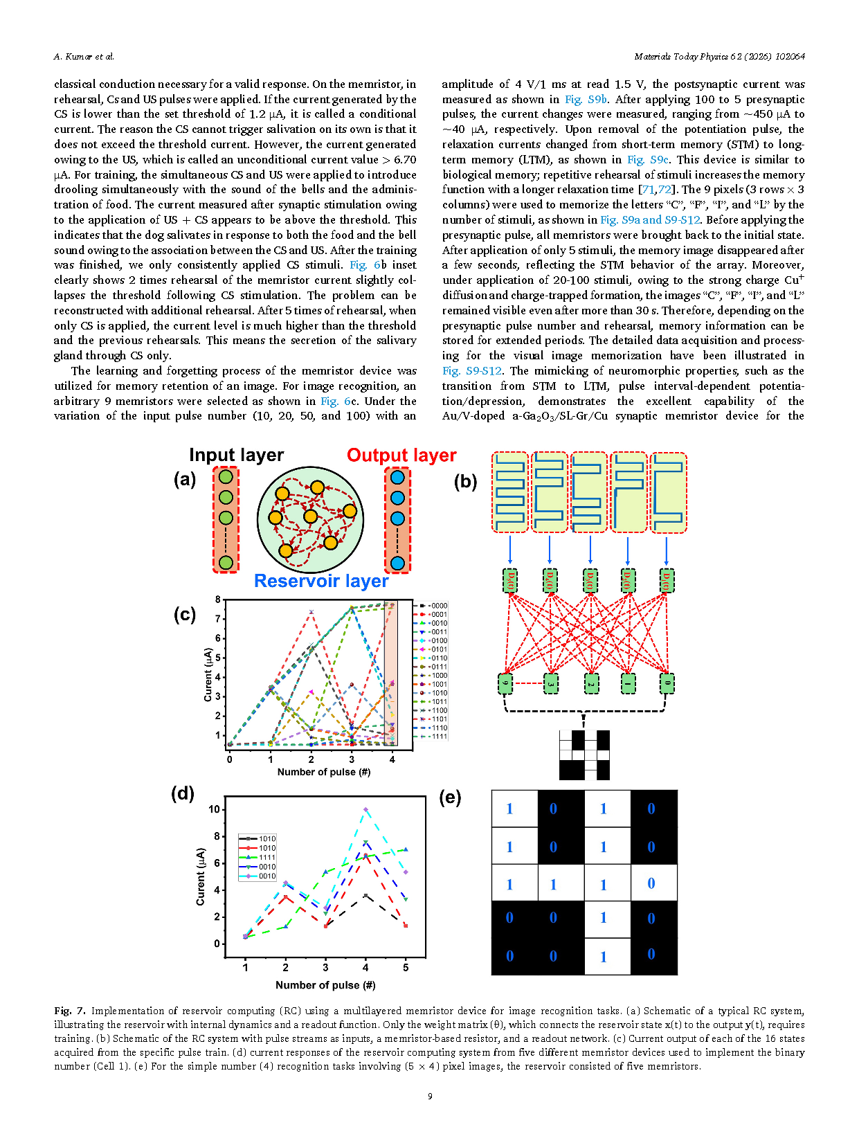
Fig. 7. Implementation of reservoir computing (RC) using a multilayered memristor device for image recognition tasks. (a) Schematic of a typical RC system, illustrating the reservoir with internal dynamics and a readout function. Only the weight matrix (θ), which connects the reservoir state x(t) to the output y(t), requires training. (b) Schematic of the RC system with pulse streams as inputs, a memristor-based resistor, and a readout network. (c) Current output of each of the 16 states acquired from the specific pulse train. (d) current responses of the reservoir computing system from five different memristor devices used to implement the binary number (Cell 1). (e) For the simple number (4) recognition tasks involving (5 × 4) pixel images, the reservoir consisted of five memristors.
DOI:
doi.org/10.1016/j.mtphys.2026.102064