


Member News
【Member News】Breakthrough of 9,000 V! Jiufengshan Laboratory Sets New Breakdown Voltage Record for Ga₂O₃ MOSFETs
日期:2026-03-31阅读:245
Recently, Jiufengshan Laboratory has achieved a major breakthrough in the field of ultra-wide bandgap semiconductors, successfully developing a lateral Ga₂O₃ MOSFET with a breakdown voltage exceeding 9,000 V based on domestically produced homoepitaxial wafers. This milestone signifies that the laboratory has reached an internationally advanced level in ultra-high-voltage Ga₂O₃ power device technology.
9,000 V: A New World Record for Ga₂O₃ Breakdown Voltage
Ga₂O₃, with its ultra-wide bandgap (~4.8 eV) and high critical electric field (~8 MV/cm), is widely regarded as an ideal material for next-generation high-voltage power devices. However, due to limitations in materials and fabrication processes, previously reported Ga₂O₃ MOSFETs typically exhibited breakdown voltages below 4,000 V.
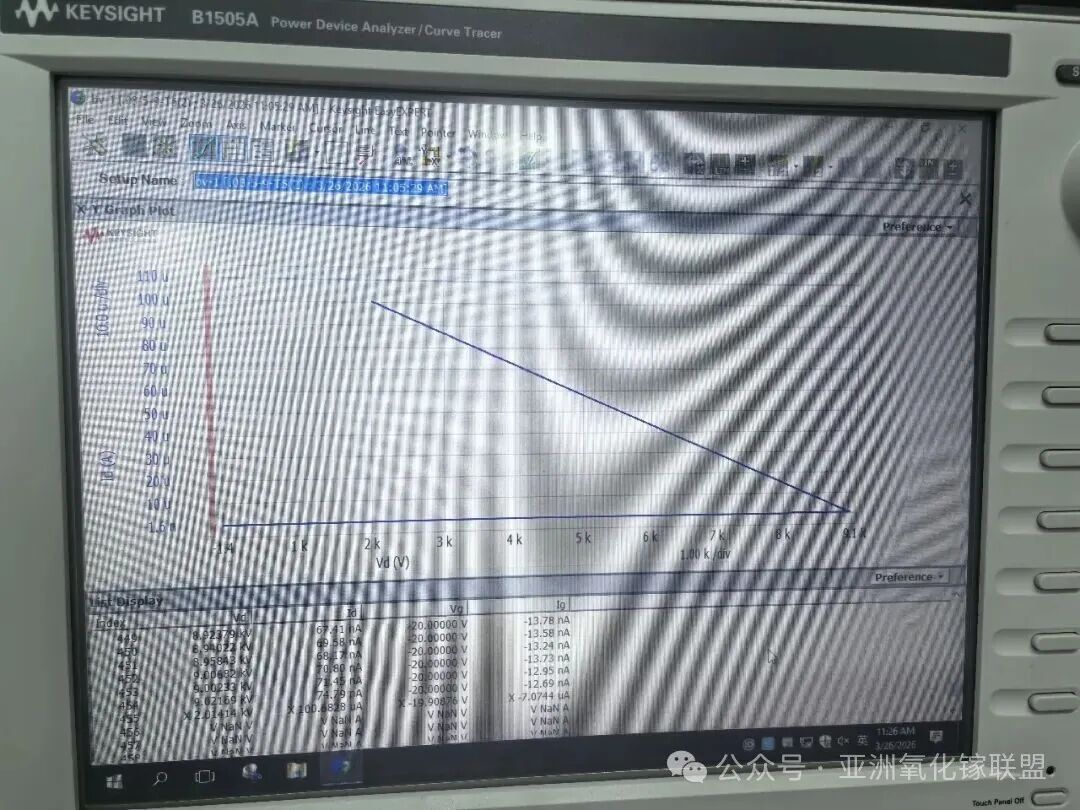
Through a double-layer source field plate design, the Jiufengshan Laboratory team effectively modulated the internal electric field distribution, achieving a breakdown voltage of 9.02 kV. Under test conditions of VGS = 5 V and VDS = 10 V, the device demonstrated a forward current of 120 μA, validating the strong potential of Ga₂O₃ in ultra-high-voltage power electronics applications.
Homoepitaxy + Non-p-Type Heterostructure: A Synergistic Breakthrough
This achievement addresses two key challenges:
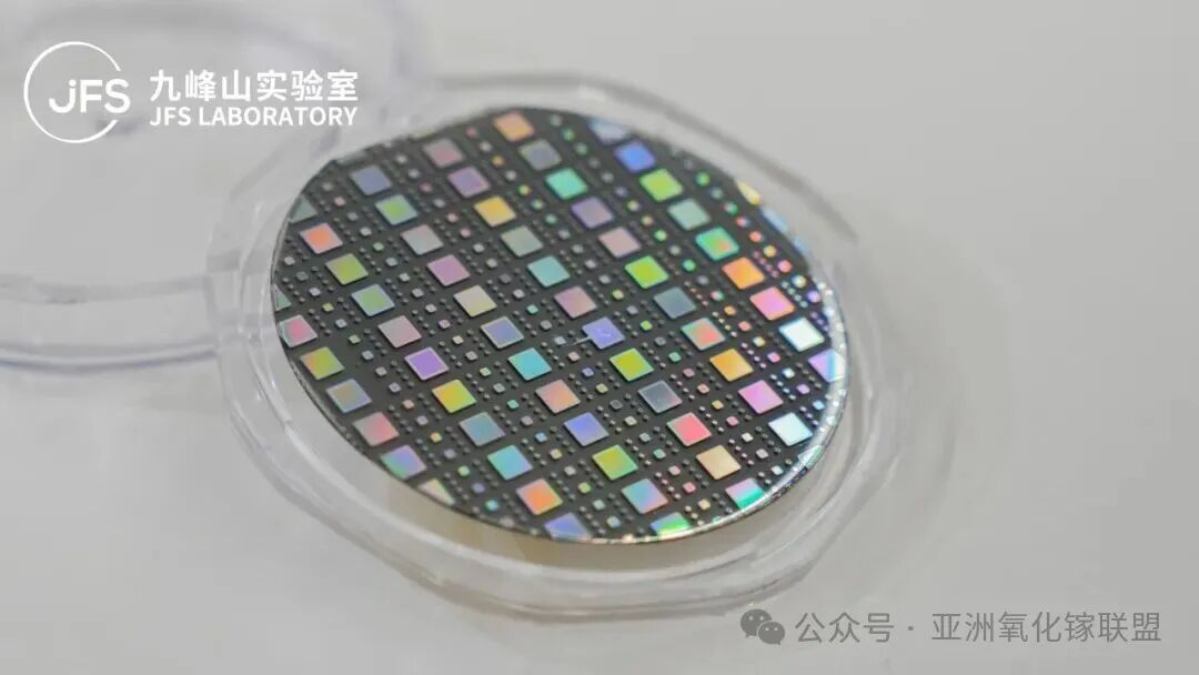
Use of domestically produced homoepitaxial wafers:The device is based on locally developed Ga₂O₃ homoepitaxial materials, enabling the breakdown voltage to reach 9.02 kV and providing a technologically independent solution for high-voltage and high-frequency applications.
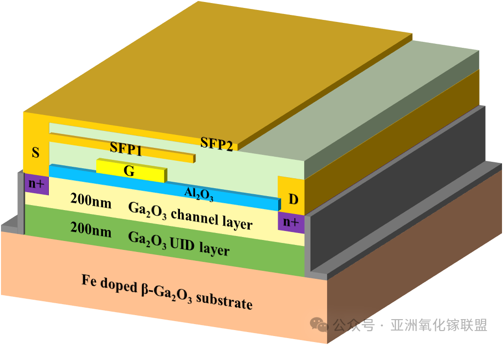
Adoption of a non-p-type heterostructure design:Unlike conventional approaches that rely on p-type oxides, this device avoids such structures entirely. Instead, it leverages a double field plate design to bypass issues related to lattice mismatch and the instability of p-type oxides, fully exploiting the intrinsic high breakdown strength of Ga₂O₃.
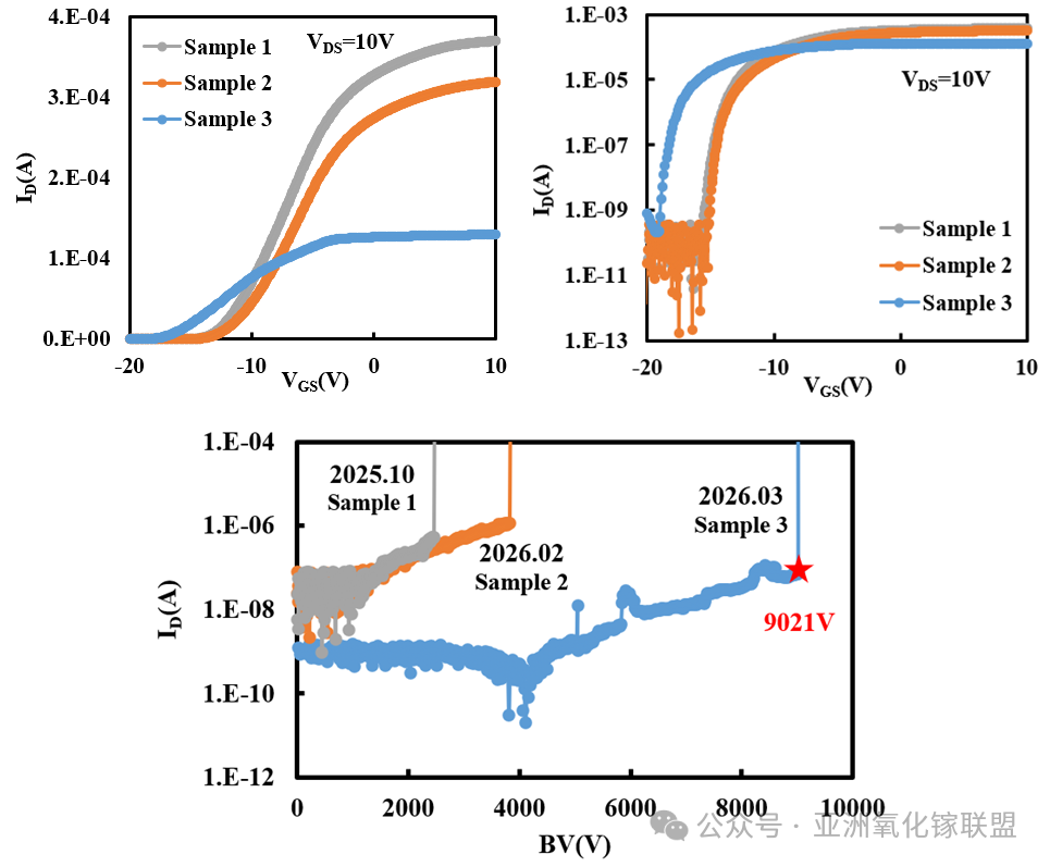
Experimental data show that the lateral MOSFET achieves a forward current of 120 μA at VGS = 5 V and VDS = 10 V, with a breakdown voltage of 9.02 kV, confirming the effectiveness of this structure in enabling ultra-high-voltage performance.
From Accumulation to Breakthrough: Leading Global Patent Positioning
Beyond technical innovation, intellectual property plays a crucial role. According to the Ga₂O₃ Patent Technology Analysis published by the Patent Examination Cooperation Beijing Center of the China National Intellectual Property Administration, Jiufengshan Laboratory has established a comprehensive patent portfolio in Ga₂O₃ device technologies, ranking among the global leaders and providing strong support for China’s technological independence in fourth-generation semiconductors.
Jiufengshan Laboratory remains committed to building an open innovation ecosystem for compound semiconductors. It currently offers capabilities in Ga₂O₃ device R&D and fabrication, including Ga₂O₃ substrates and epitaxial wafers, research-grade discrete devices, and foundry services—supporting partners in accelerating innovation in the fourth-generation semiconductor landscape.
