Paper Sharing
【Domestic Papers】A megawatt ultra-wide bandgap semiconductor module for pulsed power electronics
日期:2026-03-31阅读:214
Researchers from the University of Hong Kong, Virginia Polytechnic Institute and State University, Nanjing University have published a dissertation titled "A megawatt ultra-wide bandgap semiconductor module for pulsed power electronics" in Nature Communications.
Background
Power semiconductor devices are central components in power electronics systems for consumer electronics, data centers, electric vehicles, renewable energy processing, and electric grids, with a global market exceeding US$50 billion. In the past two decades, wide-bandgap (WBG) semiconductors such as gallium nitride (GaN) and silicon carbide (SiC) have outperformed conventional silicon (Si) devices. Recently, ultra-wide bandgap (UWBG) semiconductors including gallium oxide (Ga₂O₃), aluminum nitride (AlN), and diamond have emerged as promising candidates for next-generation power devices, owing to their higher critical electric field and thermal stability, with Baliga’s figure of merit at least 3.8 times that of GaN/SiC and 3000 times that of Si.
Over the past decade, the power level of UWBG devices has advanced to the kilowatt scale but still fails to meet the megawatt (MW)-level pulsed power demands in industrial, biomedical, grid, and aerospace applications. Conventional large-area devices are limited by material non-uniformity, defects, and fabrication variability, leading to a trade-off between breakdown voltage and forward current. Moreover, UWBG device packaging faces challenges of high electric fields, high heat fluxes, and low thermal conductivity, and no practical multi-die power module has been demonstrated, resulting in a long-term power level stagnation.
This work addresses the power scaling bottleneck of UWBG devices through device-package electrothermal co-design and explores their application in pulsed power electronics.
Abstract
Ultra-wide bandgap semiconductors exhibit advantageous electronic properties that make them promising for high-voltage, high-power electronics applications. Building on over a decade of progress in material growth and device fabrication, discrete ultra-wide bandgap devices with power-switching capacities up to the kilowatt level have been recently demonstrated. However, a packaged, multi-die ultra-wide bandgap power module – essential for further power scaling toward industrial, biomedical, grid, and aerospace applications – has yet to be realized. Here, we present a flip-chip packaged gallium oxide power module capable of 1000 A, 1000 V pulsed power switching with fast speed and minimal reverse recovery, advancing the power capacity of ultra-wide bandgap electronics by over two orders of magnitude. To address challenges posed by high electric fields and transient power surges, we employ a high-permittivity interface design enabling device-package electrothermal co-optimization. This optimization maximizes the module’s transient thermal performance and enables full exploitation of the high volumetric heat capacity of gallium oxide—a largely untapped advantage in prior device development—alongside its high-temperature stability. The optimized ultra-wide bandgap module achieves over 1.8 MW/cm² pulsed power capacity density, outperforming silicon and wide-bandgap semiconductor counterparts and suggesting the promise of ultra-wide bandgap electronics in next-generation high-power systems.
Highlights
Module Performance Breakthrough:First demonstration of a UWBG multi-die power module with 1000 V/1000 A megawatt-level pulsed switching, advancing power capacity by over two orders of magnitude.
Innovative Interface Design:High-permittivity BaTiO₃ interface replaces conventional posts, effectively suppressing electric field crowding and reducing thermal resistance by more than 50%.
Material Advantage Exploitation:Full utilization of Ga₂O₃’s high volumetric heat capacity and high-temperature stability, resulting in lower temperature rise and higher current handling under short pulses.
Electrothermal Co-optimization:Device-package co-design achieves high-voltage blocking, large-current conduction, and efficient heat dissipation, adapting to transient pulsed power conditions.
Reliability Improvement:Optimized interface enhances thermomechanical matching, with minimal performance degradation after 10,000 power-cycling tests, significantly boosting stability.
Conclusion
This work demonstrates a multi-die, device-package co-optimized Ga₂O₃ module capable of continuous pulsed power switching at 1000 A, 1000 V with fast switching speed and minimal reverse recovery, setting a record power capacity among UWBG power devices. A high-κ interface design is deployed to replace the conventional post in the JSC package, resulting in over 50% reduction in thermal resistance while enabling >2 kV avalanche breakdown operation at temperatures up to 250 ℃. Leveraging the high Cᵥ of Ga₂O₃, the intrinsic thermal stability of Ga₂O₃ devices, and the electrothermally co-optimized package design, the Ga₂O₃ module surpasses Si and WBG counterparts in power capacity density. These findings offer guidance for material selection and packaging strategies in high-power pulsed applications and provide a valuable reference point for module development and power scaling across emerging WBG and UWBG materials.
Looking forward, further upscaling of Ga₂O₃ devices and modules toward higher power capacity will require concurrent advances in current and voltage ratings, as well as high-voltage reliability at temperatures beyond the 250 ℃ demonstrated here. From a material perspective, this calls for the development of larger-diameter Ga₂O₃ wafers with improved uniformity and reduced defect density, together with thicker and low-doped epitaxial layers to support higher voltages. At the device and module levels, continued optimization of edge terminations and heterogeneous interfaces in both devices and packaging will be essential to alleviate degradation mechanisms accelerated by the combined effects of high electric field and elevated temperature. Beyond diode demonstrations, the realization of Ga₂O₃ transistors that leverage the device-package co-design principles identified in this work will be critical for enabling fully integrated, all-Ga₂O₃ pulsed-power systems.
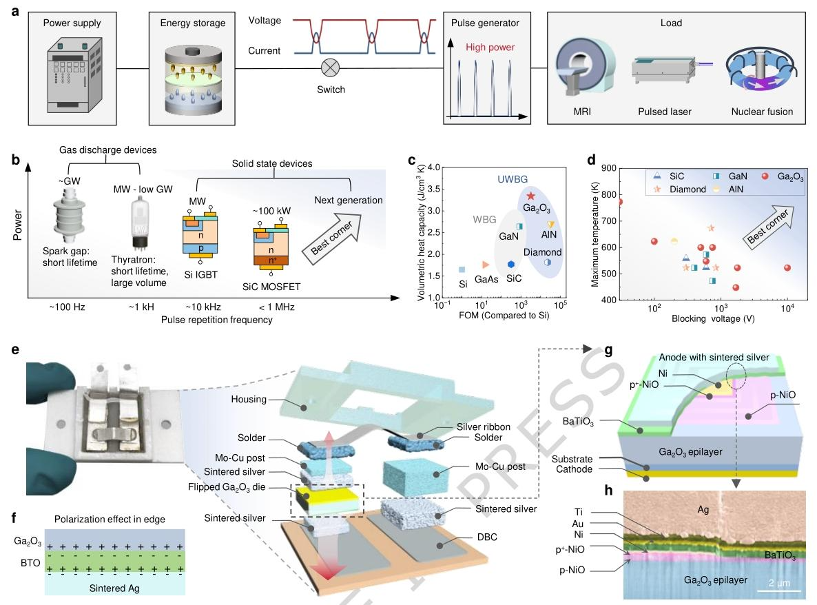
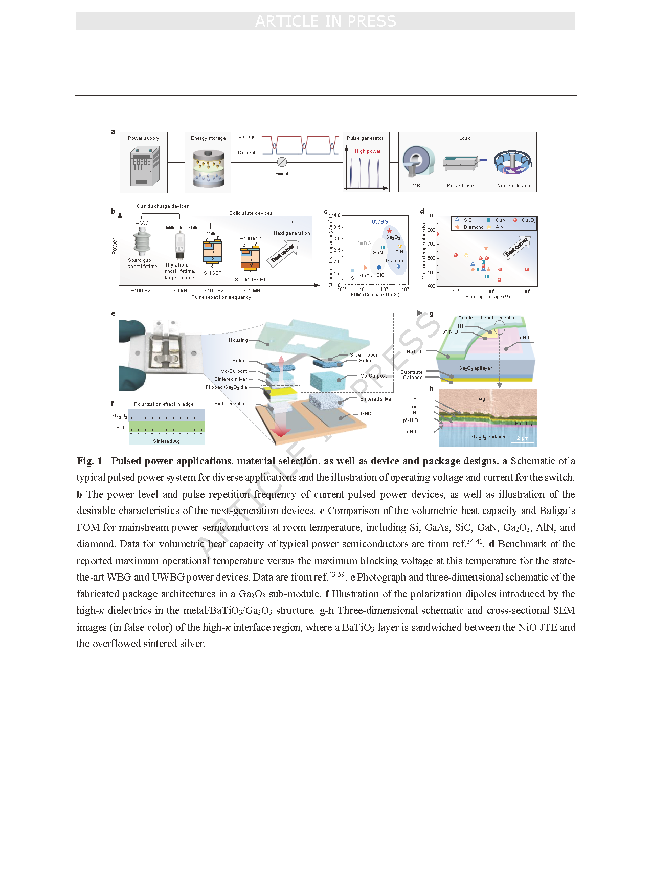
Fig. 1 | Pulsed power applications, material selection, as well as device and package designs. a Schematic of a typical pulsed power system for diverse applications and the illustration of operating voltage and current for the switch. b The power level and pulse repetition frequency of current pulsed power devices, as well as desirable characteristics of the next-generation devices. c Comparison of the volumetric heat capacity and Baliga’s FOM for mainstream power semiconductors at room temperature, including Si, GaAs, SiC, GaN, Ga₂O₃, AlN, and diamond. Data for volumetric heat capacity of typical power semiconductors are from ref.34–41. d Benchmark of the maximum operational temperature versus the maximum blocking voltage at this temperature for the state-of-the-art WBG and UWBG power devices. Data are from ref.43–59. e Photograph and three-dimensional schematic of the reported package architectures in a Ga₂O₃ sub-module. f Illustration of the polarization dipoles introduced by the high-κ dielectrics in the metal/BaTiO₃/Ga₂O₃ structure. g–h Three-dimensional schematic and cross-sectional SEM images (in false color) of the high-κ interface region, where a BaTiO₃ layer is sandwiched between the NiO JTE and the overflowed sintered silver.
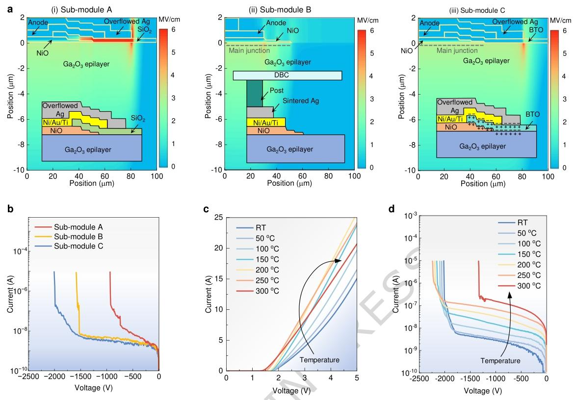
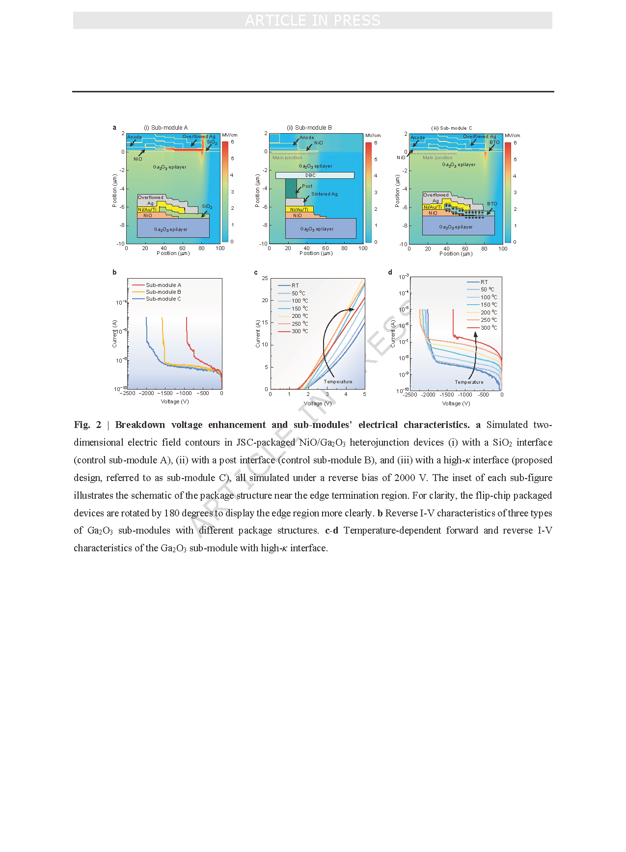
Fig. 2 | Breakdown voltage enhancement and sub-modules’ electrical characteristics. a Simulated two-dimensional electric field contours in JSC-packaged NiO/Ga₂O₃ heterojunction devices (i) with a SiO₂ interface (control sub-module A), (ii) with a post interface (control sub-module B), and (iii) with a high-κ interface (proposed design, referred to as sub-module C), all simulated under a reverse bias of 2000 V. The inset of each sub-figure illustrates the schematic of the package structure near the edge termination region. For clarity, the flip-chip packaged devices are rotated by 180 degrees to display the edge region more clearly. b Reverse I–V characteristics of three types of Ga₂O₃ sub-modules with different package structures. c–d Temperature-dependent forward and reverse I–V characteristics of the Ga₂O₃ sub-module with high-κ interface.
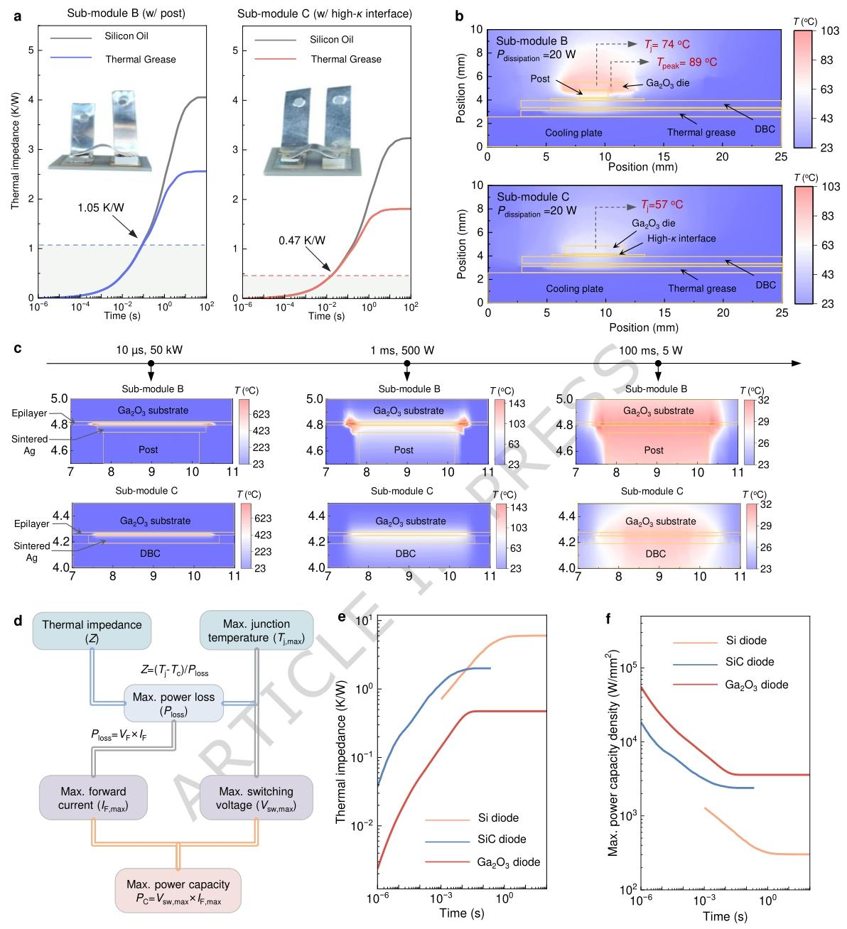
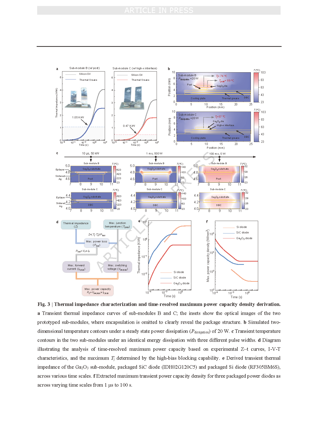
Fig. 3 | Thermal impedance characterization and time-resolved maximum power capacity density derivation. a Transient thermal impedance curves of sub-modules B and C; the insets show the optical images of the two prototyped sub-modules, where encapsulation is omitted to clearly reveal the package structure. b Simulated two-dimensional temperature contours under a steady state power dissipation (Pdissipation) of 20 W. c Transient temperature contours in the two sub-modules under an identical energy dissipation with three different pulse widths. d Diagram illustrating the analysis of time-resolved maximum power capacity based on experimental Z~t curves, I–V–T characteristics, and the maximum Tⱼ determined by the high-bias blocking capability. e Derived transient thermal impedance of the Ga₂O₃ sub-module, packaged SiC diode (IDH02G120C5) and packaged Si diode (RF305BM6S), across various time scales. f Extracted maximum transient power capacity density for three packaged power diodes as across varying time scales from 1 µs to 100 s.
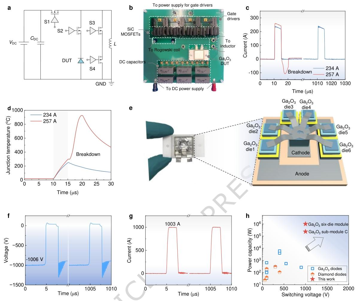
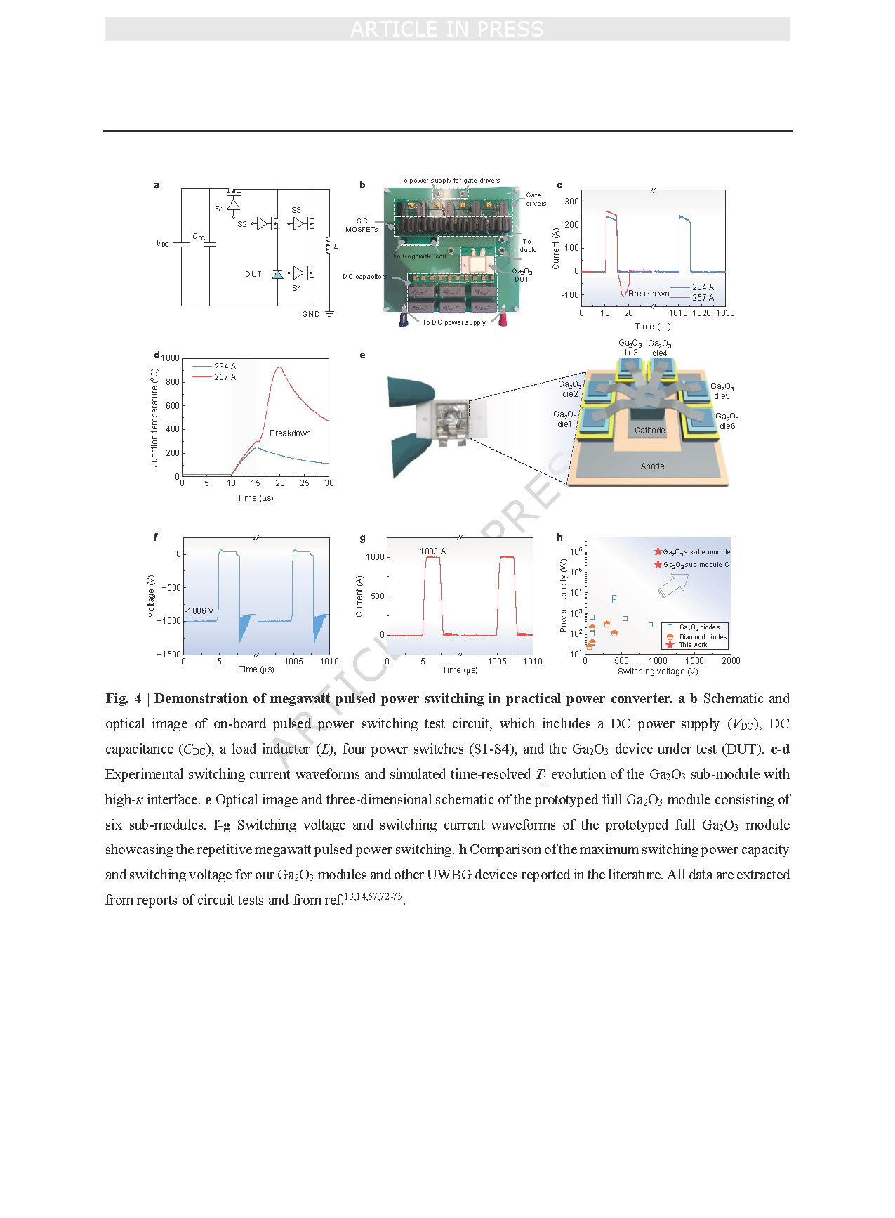
Fig. 4 | Demonstration of megawatt pulsed power switching in practical power converter. a–b Schematic and optical image of on-board pulsed power switching test circuit, which includes a DC power supply (VDC), DC capacitance (CDC), a load inductor (L), four power switches (S1–S4), and the Ga₂O₃ device under test (DUT). c–d Experimental switching current waveforms and simulated time-resolved Tⱼ evolution of the Ga₂O₃ sub-module with high-κ interface. e Optical image and three-dimensional schematic of the prototyped full Ga₂O₃ module consisting of six sub-modules. f–g Switching voltage and switching current waveforms of the prototyped full Ga₂O₃ module showcasing the repetitive megawatt pulsed power switching. h Comparison of the maximum switching power capacity and switching voltage for our Ga₂O₃ modules and other UWBG devices reported in the literature.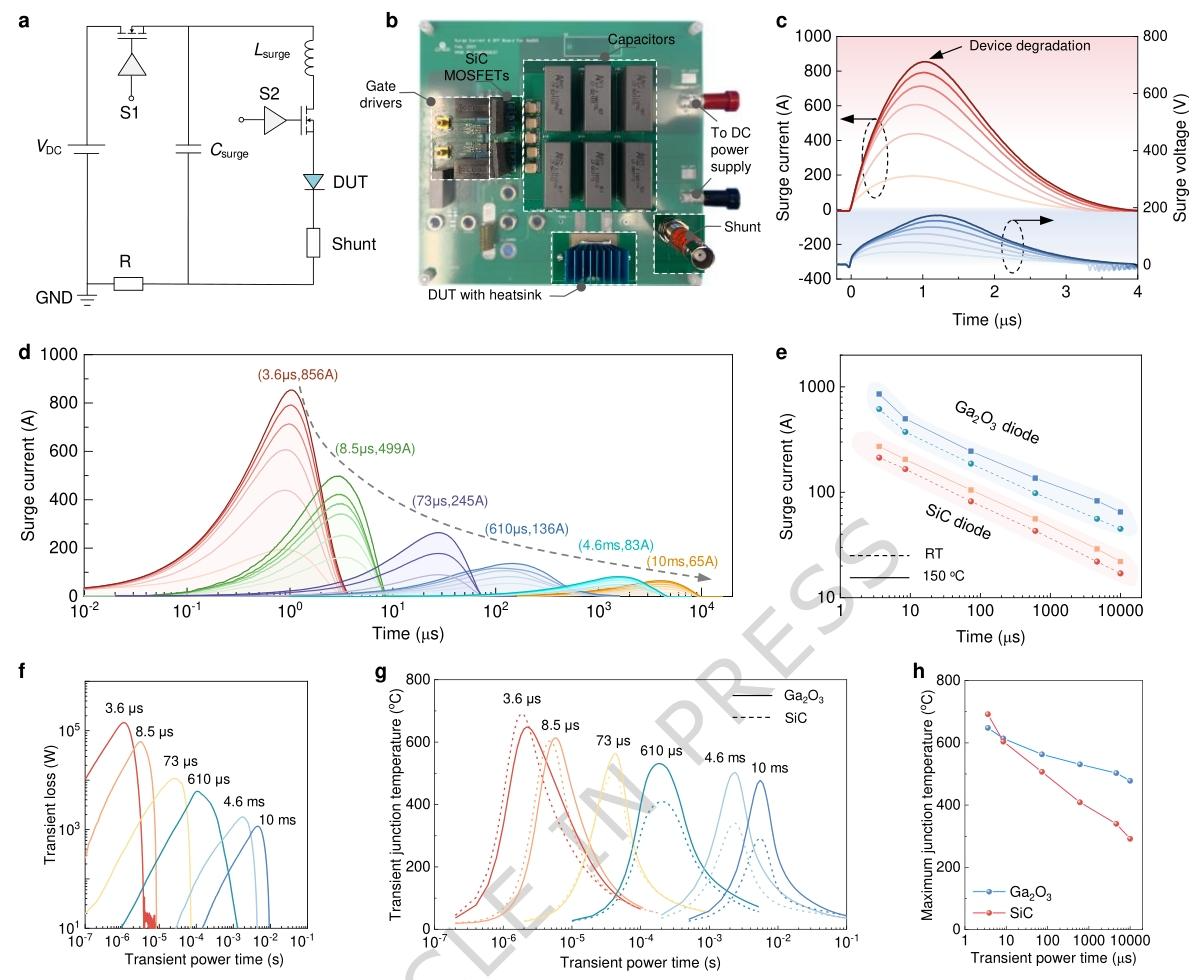
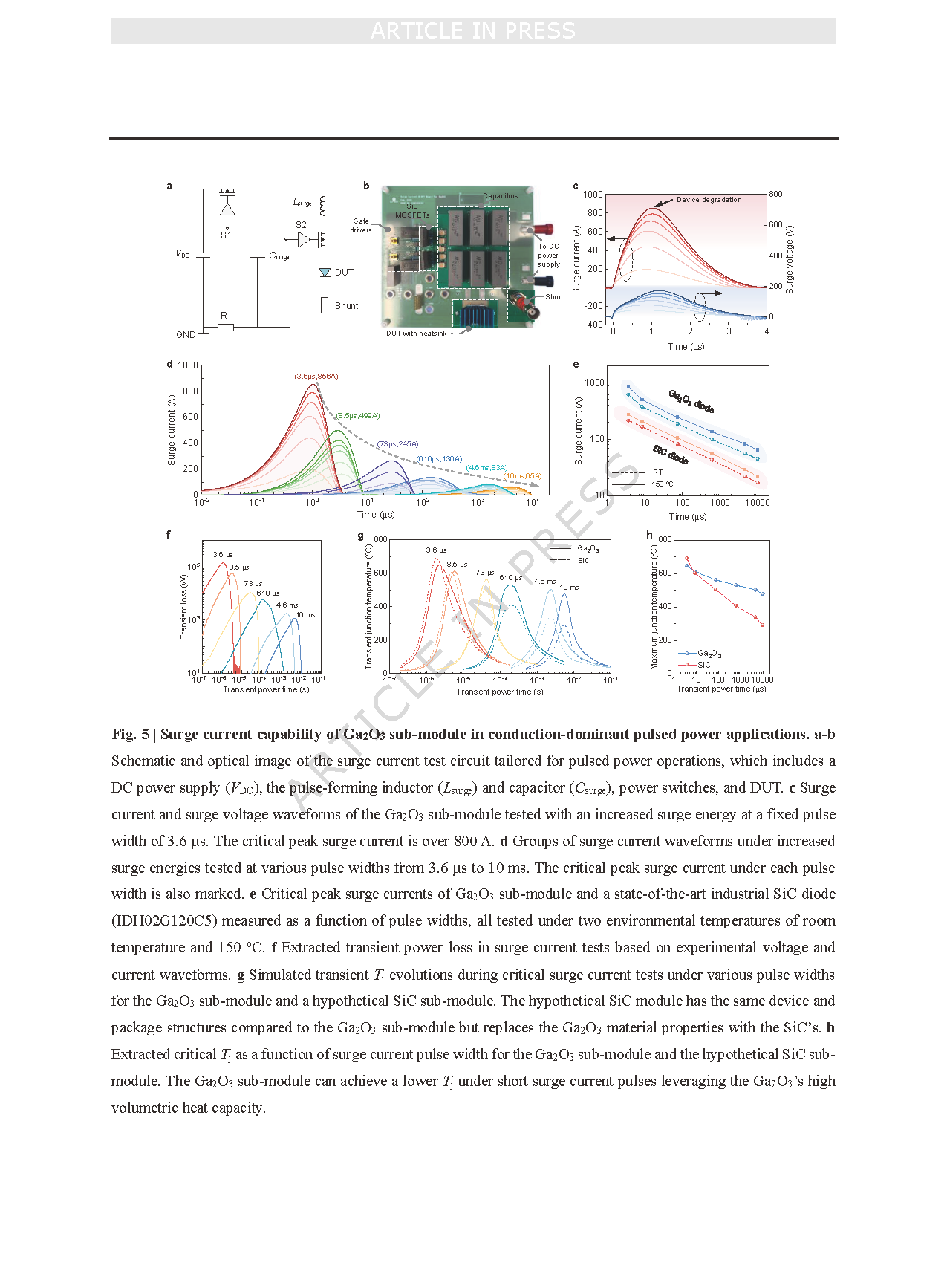
Fig. 5 | Surge current capability of Ga₂O₃ sub-module in conduction-dominant pulsed power applications. a–b Schematic and optical image of the surge current test circuit tailored for pulsed power operations, which includes a DC power supply (VDC), the pulse-forming inductor (Lsurge) and capacitor (Csurge), power switches, and DUT. c Surge current and surge voltage waveforms of the Ga₂O₃ sub-module tested with an increased surge energy at a fixed pulse width of 3.6 µs. The critical peak surge current is over 800 A. d Groups of surge current waveforms under increased surge energies tested at various pulse widths from 3.6 µs to 10 ms. The critical peak surge current under each pulse width is also marked. e Critical peak surge currents of Ga₂O₃ sub-module and a state-of-the-art industrial SiC diode (IDH02G120C5) measured as a function of pulse widths, all tested under two environmental temperatures of room temperature and 150 ℃. f Extracted transient power loss in surge current tests based on experimental voltage and current waveforms. g Simulated transient Tⱼ evolutions during critical surge current tests under various pulse widths for the Ga₂O₃ sub-module and a hypothetical SiC sub-module. The hypothetical SiC module has the same device and package structures compared to the Ga₂O₃ sub-module but replaces the Ga₂O₃ material properties with the SiC’s. h Extracted critical Tⱼ as a function of surge current pulse width for the Ga₂O₃ sub-module and the hypothetical SiC sub-module. The Ga₂O₃ sub-module can achieve a lower Tⱼ under short surge current pulses leveraging the Ga₂O₃’s high volumetric heat capacity.
DOI:
doi.org/10.1038/s41467-026-71274-6