Paper Sharing
【International Papers】Atomic layer deposition of gallium oxide using gallium triazenide and water
日期:2026-03-30阅读:159
Researchers from the Linköping University have published a dissertation titled " Atomic layer deposition of gallium oxide using gallium triazenide and water " in Materials Advances.
Background
Wide-bandgap (WBG) semiconductors provide orders-of-magnitude higher breakdown fields and lower carrier leakage than Si. Breakthroughs in the 1990s–2000s, notably with silicon carbide (SiC) and gallium nitride (GaN), enabled high-voltage Schottky diodes, metal-oxide-semiconductor field-effect transistors (MOSFETs) and high-electron-mobility transistors (HEMTs), all of which are now widely used in electric-vehicle inverters, server power supplies, and radio-frequency amplifiers. Over the past decade, attention has shifted to ultra-wide-bandgap (UWBG) materials (bandgaps >4 eV), because they promise greater performance gains. This subclass includes β-gallium oxide (β-Ga2O3), diamond, and aluminium nitride. The wider bandgaps of WBG and UWBG semiconductors, relative to Si, yield exponentially lower intrinsic carrier concentrations, and enable high-temperature operation. Their high critical breakdown fields also allow devices to block high voltages with thinner, more heavily doped drift layers, dramatically reducing on-state losses. Direct-bandgap UWBG materials are strongly transparent in the deep UV-region, making them suitable for solar-blind photodetectors and other related optical devices. β-Ga2O3 has an optical bandgap of 4.8 eV (absorption edge ≈255 nm), rendering it solar-blind (insensitive above ∼280 nm) and attractive for UV photodetectors and optical coatings. Stoichiometric, highly pure β-Ga2O3 films are typically clear and highly transparent, however, O-vacancies and impurities can impart yellowish or bluish tints. The ability to tune these optical features by controlling film composition is advantageous for UV-sensor and filter applications.
Abstract
Gallium oxide (Ga2O3) is an ultrawide bandgap semiconductor with promising applications in power electronics and UV-photodetectors. Herein, we present thermal atomic layer deposition (ALD) of Ga2O3 thin films using tris(1,3-diisopropyltriazenide)gallium(III) and water. The deposition process shows saturation in the growth per cycle of ∼1.5 Å at precursor pulses ≥2 s with a narrow ALD temperature interval between 400 and 415 °C, and a nucleation delay of ∼15 cycles. Time-of-flight elastic recoil detection analysis revealed near-stoichiometric Ga2O3 with <3.5 at%, of C, H, N, and Cl, all of which decreases after annealing. Grazing Incidence X-ray diffraction reveals that annealing at 700 °C converts as-deposited amorphous films into phase-pure β-Ga2O3. The as-deposited films were highly transparent (>96%) with an optical bandgap of ∼3.74 eV, which increased to ∼4.0 eV upon annealing. Electrical conductivity also increased from ∼3 mS cm−1 in the as deposited films to ∼30 mS cm−1 after annealing. This work extends the ALD chemistry of triazenide precursors, previously validated for GaN, InN, InGaN and In2O3, to Ga2O3.
Conclusion
This work demonstrates ALD of Ga2O3 using Ga(triaz)3 with water. Saturation behaviour was observed with precursor pulse durations ≥2 s, yielding a GPC of ∼1.5 Å. The process exhibited a narrow ALD temperature interval between 400 and 415 °C, and film thickness scaled linearly with cycle count after a ∼15 cycles nucleation delay. Ga(triaz)3 showed reactivity comparable to Ga trialkyl, halide, and alkoxide precursors used in conventional thermal ALD. As-deposited films were near-stoichiometric but contained minor C, H, N, and Cl (precursor derived), and Cu from hardware. Annealing reduced these impurities and increased the O : Ga ratio to ∼1.6–1.7. Cl levels remained minimal throughout, highlighting the effectiveness of precursor purification and ligand design. As a result, the films produced here rank among the purest reported for thermal ALD of Ga2O3 using water as the O-source. GI-XRD confirmed amorphous as-deposited films crystallized to monoclinic β-Ga2O3 after annealing at 700 °C. Optically, transmittance exceeded 96% in the as-deposited state and decreased by ∼10% after annealing, and Tauc plots showed the bandgap increasing from ∼3.74 to 4.00 eV. Electrically, all films exhibit higher conductivity after annealing, consistent with β-phase formation and improved structural order. Taken together, XRD and ToF-ERDA corroborated that the property changes arised from crystallization, reduced defect/ligand residues, and a modest shift toward O-richer composition.
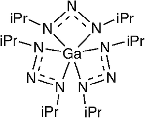
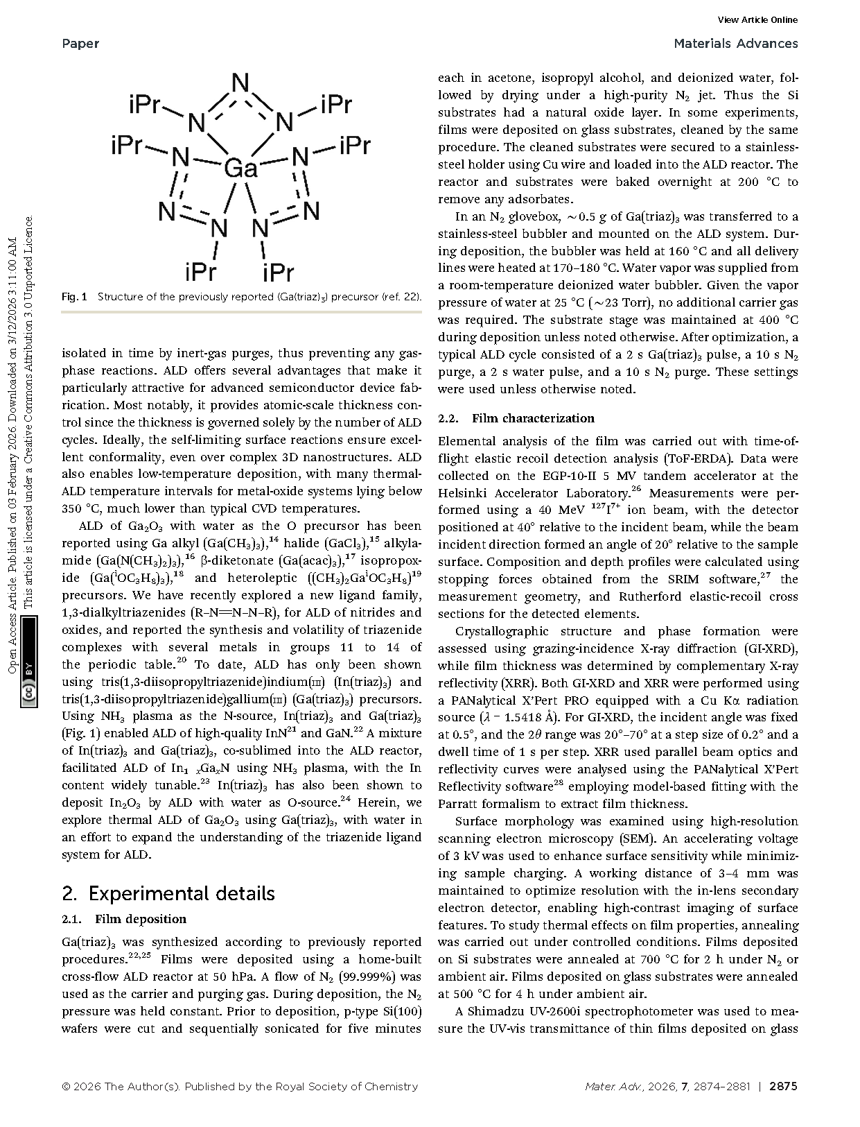
Fig. 1. Structure of the previously reported (Ga(triaz)3) precursor.
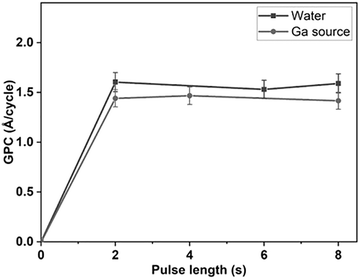
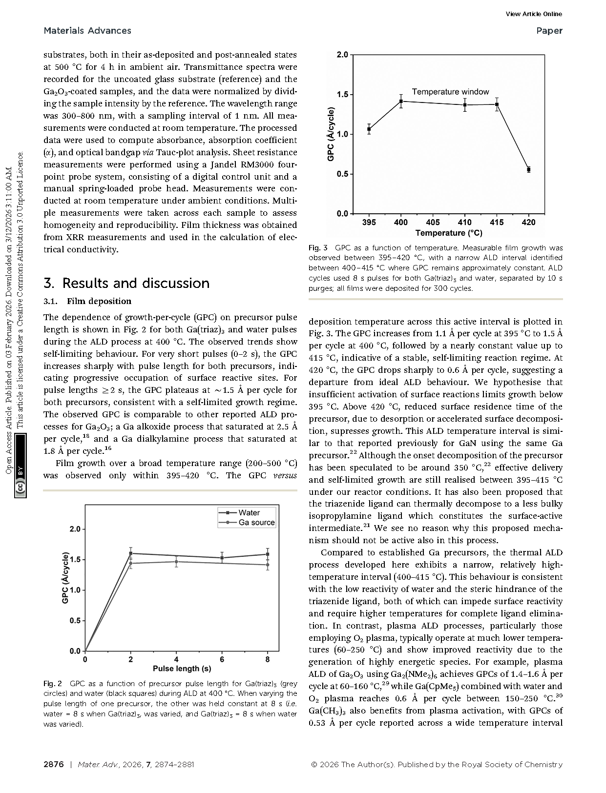
Fig. 2. GPC as a function of precursor pulse length for Ga(triaz)3 (grey circles) and water (black squares) during ALD at 400 °C. When varying the pulse length of one precursor, the other was held constant at 8 s (i.e. water = 8 s when Ga(triaz)3, was varied, and Ga(triaz)3 = 8 s when water was varied).
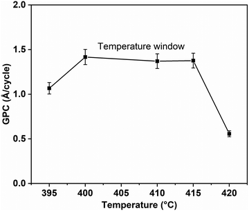
Fig. 3. GPC as a function of temperature. Measurable film growth was observed between 395–420 °C, with a narrow ALD interval identified between 400–415 °C where GPC remains approximately constant. ALD cycles used 8 s pulses for both Ga(triaz)3 and water, separated by 10 s purges; all films were deposited for 300 cycles.
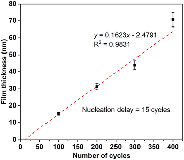
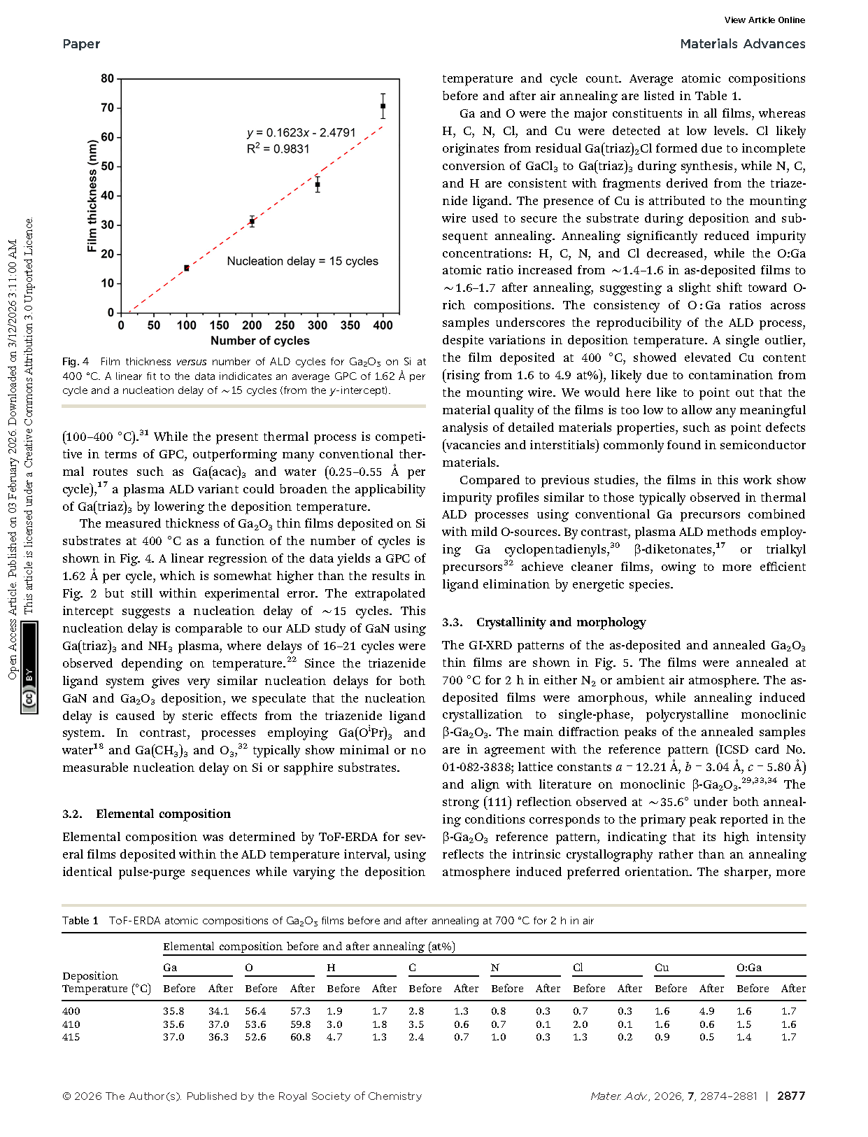
Fig. 4. Film thickness versus number of ALD cycles for Ga2O3 on Si at 400 °C. A linear fit to the data indidicates an average GPC of 1.62 Å per cycle and a nucleation delay of ∼15 cycles (from the y-intercept).
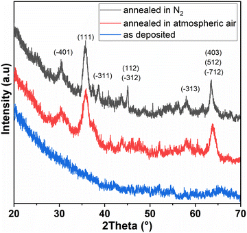
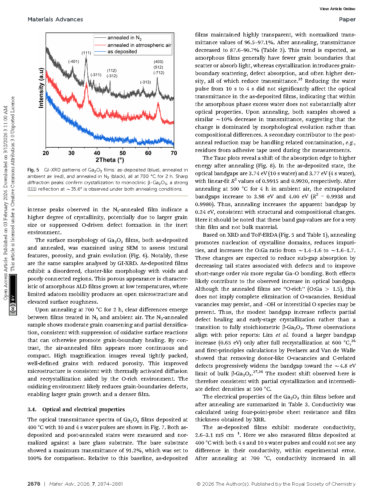
Fig. 5. GI-XRD patterns of Ga2O3 films: as-deposited (blue), annealed in ambient air (red), and annealed in N2 (black), all at 700 °C for 2 h. Sharp diffraction peaks confirm crystallization to monoclinic β-Ga2O3; a strong (111) reflection at ∼35.6° is observed under both annealing conditions.
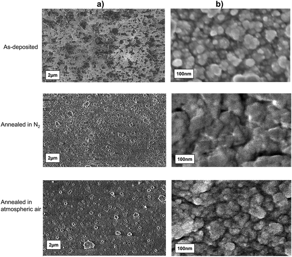
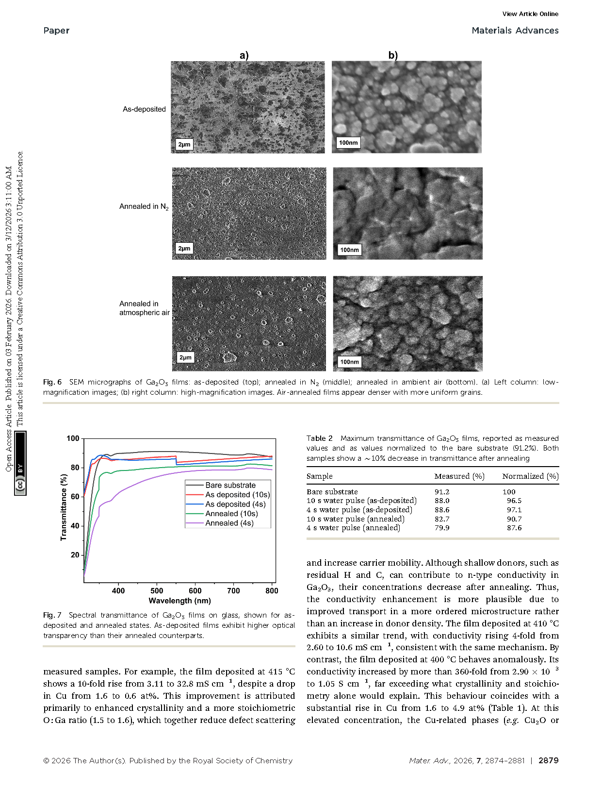
Fig. 6. SEM micrographs of Ga2O3 films: as-deposited (top); annealed in N2 (middle); annealed in ambient air (bottom). (a) Left column: low-magnification images; (b) right column: high-magnification images. Air-annealed films appear denser with more uniform grains.
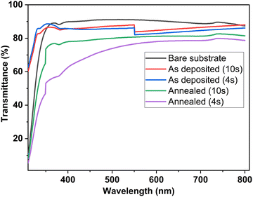
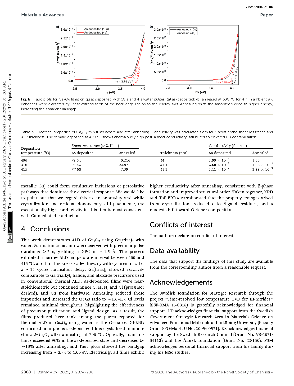
Fig. 7. Spectral transmittance of Ga2O3 films on glass, shown for as-deposited and annealed states. As-deposited films exhibit higher optical transparency than their annealed counterparts.
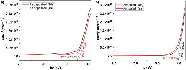
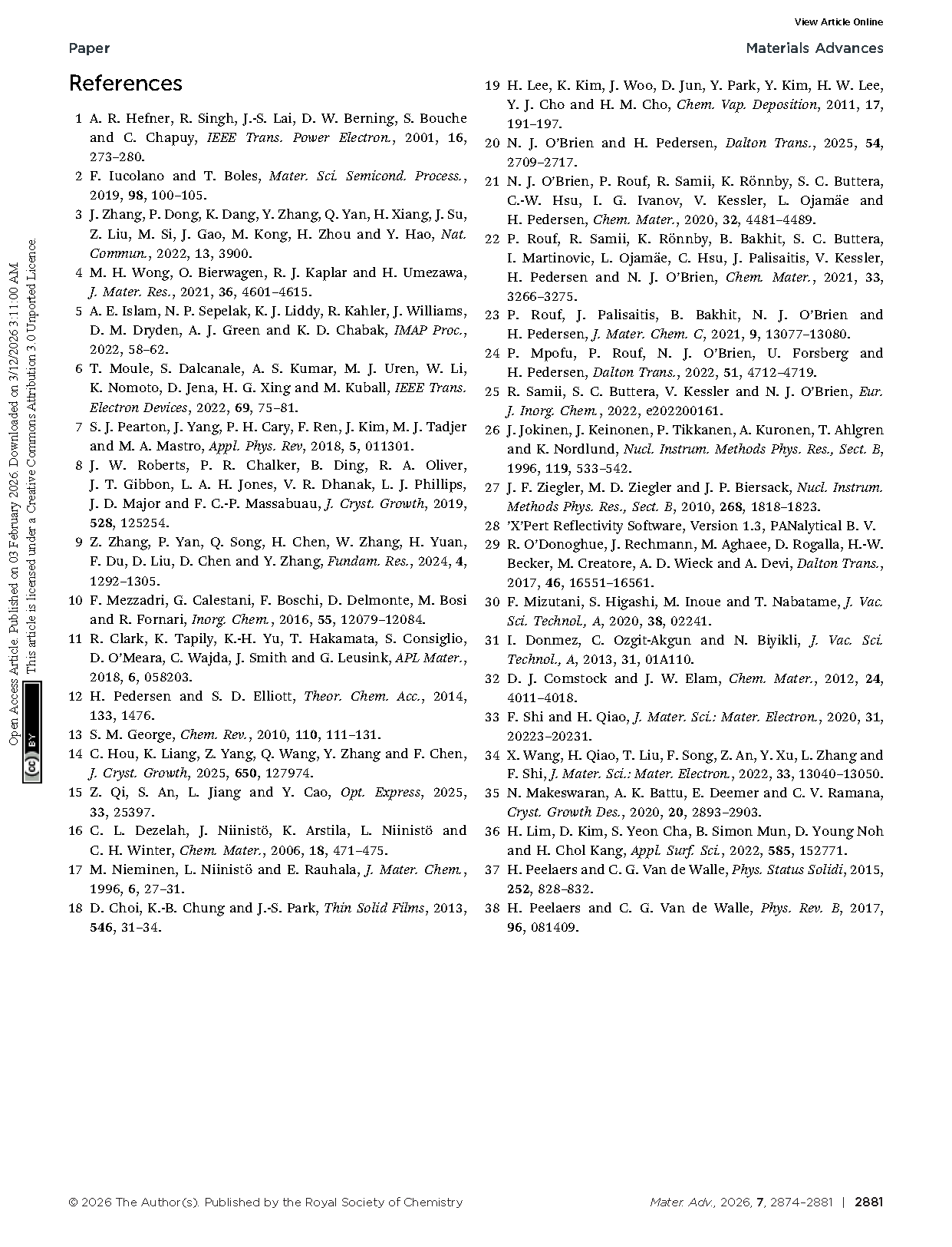
Fig. 8. Tauc plots for Ga2O3 films on glass deposited with 10 s and 4 s water pulses: (a) as-deposited; (b) annealed at 500 °C for 4 h in ambient air. Bandgaps were extracted by linear extrapolation of the near-edge region to the energy axis. Annealing shifts the absorption edge to higher energy, increasing the apparent bandgap.
DOI:
doi.org/10.1039/D5MA01213A