


Member News
【Member News】World’s First 12-inch Ga₂O₃ Single Crystal Achieved, Advancing 4th-Generation Semiconductors
日期:2026-03-27阅读:324
In the opening year of the “15th Five-Year Plan,” Fujia Gallium has once again achieved a historic breakthrough!
On March 26, Fujia Gallium announced the world’s first successful fabrication of a 12-inch Gallium Oxide (Ga₂O₃) single crystal. This follows the company’s successful production of 8-inch Gallium Oxide crystals in December 2025, marking another major technological milestone. This achievement not only sets a new global record for the largest Gallium Oxide single crystal but also signifies a decisive step forward for China in the industrialization of core materials for fourth-generation semiconductors. With this, Fujia Gallium has become the first company in the world to master the technology for growing 12-inch Gallium Oxide single crystals.
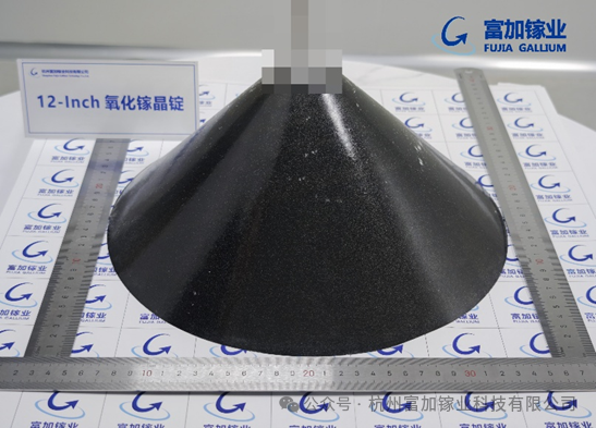
Fujia Gallium Achieves 12-Inch Gallium Oxide (305mm Diameter) Single Crystal Breakthrough
Gallium Oxide (Ga₂O₃) is a representative material in the fourth-generation semiconductor field. Thanks to its outstanding high-voltage tolerance, low energy loss, and radiation resistance, it has broad application prospects in data centers, new energy, 6G communications, controlled nuclear fusion, smart grids, rail transportation, and aerospace. The national “15th Five-Year Plan” clearly emphasizes the need to “promote the industrialization of ultra-wide bandgap semiconductors such as Gallium Oxide and diamond.”
The recent breakthrough by Fujia Gallium in producing 12-inch Gallium Oxide single crystals directly responds to this national strategy, providing a solid material foundation for China’s development of “new quality productive forces” and for securing a competitive edge in future industries. It also injects strong “Chinese momentum” into the global semiconductor industry.
Wafer size is a core metric for evaluating semiconductor technology advancement and cost efficiency. Expanding from 8-inch to 12-inch wafers is not merely a matter of scaling up; it represents a strategic leap at the industrial level. A 12-inch wafer allows for a significantly larger number of chips per wafer, substantially lowering production costs and removing a key barrier to the mass-market adoption of Gallium Oxide devices. Moreover, it enables the seamless integration of future Gallium Oxide power device production into existing mature 12-inch silicon-based integrated circuit lines, greatly reducing downstream manufacturers’ equipment investment and line conversion costs, thereby accelerating industrialization at an unprecedented pace.
Next, Fujia Gallium will work closely with downstream users to conduct full-chain collaborative research covering “substrate-epitaxy-device-module,” facilitating the development of China’s high-performance Gallium Oxide power devices. This will speed up the commercialization of high-voltage, high-power Gallium Oxide power electronics and help realize the vision of “bringing high-quality materials to the world.”
Product Portfolio
Gallium Oxide Crystal Growth Equipment
Fujia Gallium has developed the world’s first EFG crystal growth system featuring a proprietary “one-click crystal growth” function, supporting 2-inch to 6-inch crystal production. The system is protected by 6 granted domestic patents and 4 international patents. Complete equipment solutions and process packages are available.
The company has also independently developed fully automated VB (Vertical Bridgman) crystal growth equipment. It was the first in China to overcome the technical bottleneck of 6-inch single-crystal growth using the VB method, enabling large-diameter bulk crystal production. This platform is supported by 6 granted domestic patents and 4 international patents, with customizable equipment and process solutions available.
Gallium Oxide Single-Crystal Substrates
As one of China’s earliest pioneers in Gallium Oxide single-crystal research and an industry-leading supplier, Fujia Gallium provides high-quality single-crystal substrates to global customers.
The product portfolio includes 26 standard substrate specifications ranging from 2-inch to 6-inch diameters. Customized solutions are available in terms of wafer size, electrical properties, and crystal orientation, supporting both advanced epitaxy R&D and volume production requirements.
Gallium Oxide Epitaxial Wafers
Built upon mature MOCVD (Metal-Organic Chemical Vapor Deposition) and MBE (Molecular Beam Epitaxy) platforms, Fujia Gallium offers 15 standard epitaxial wafer products from 2-inch to 6-inch formats, as well as customized MBE-based epitaxial structures.
The company provides integrated “substrate + epitaxy” solutions. A precise process control system enables customization of key parameters including epitaxial layer thickness, doping concentration, and compositional uniformity, meeting diverse requirements across different power levels and device architectures.
About Hangzhou Fujia Gallium
Hangzhou Fujia Gallium Technology Co., Ltd., established on December 31, 2019, is committed to the vision of “enabling the world with better materials” and focuses on the industrialization of ultra-wide bandgap Gallium Oxide semiconductor materials. Its core products include Gallium Oxide single-crystal substrates, MOCVD/MBE epitaxial wafers, and crystal growth equipment based on the Vertical Bridgman (VB) and Edge-Defined Film-Fed Growth (EFG) methods. The company provides systematic solutions for material development, accelerating the integration of the entire ultra-wide bandgap Gallium Oxide industry chain and promoting the application of Gallium Oxide materials in power devices, microwave RF devices, and optoelectronic detection. A series of major achievements in Gallium Oxide development have been featured by leading media outlets including CCTV-1, CCTV-2, People’s Daily, Xinhua News Agency, China Securities Journal, and The Paper.
In terms of corporate recognition, the company was designated as a Zhejiang Province Science and Technology SME in 2022, recognized as a National High-Tech Enterprise in 2023, and awarded the titles of Hangzhou High-Tech Enterprise R&D Center and Zhejiang “Specialized and Sophisticated” SME in 2024. In 2025, it obtained ISO 9001 Quality Management System certification (Certificate No. 20225Q20294R0M) and was also named a 2024 Hangzhou “New Eagle” Enterprise. In the Gallium Oxide field, the company is leading the drafting of the first national standard in this area and has undertaken one project from the National Development and Reform Commission and one from the Ministry of Industry and Information Technology, while participating in three additional national and provincial-level projects supported by the National Natural Science Foundation of China and regional authorities in Zhejiang and Shanghai. To date, the company has been granted 14 international patents (6 in the United States, 7 in Japan, and 1 in Europe), 42 domestic patents, three registered “Fujia Gallium” trademarks, and five software copyrights, including its proprietary “One-Click Crystal Growth” control software.
