


Member News
【Member News】GAREN SEMI Showcases World’s First 8-inch Gallium Oxide Homoepitaxial Wafer at SEMICON CHINA 2026
日期:2026-03-26阅读:257
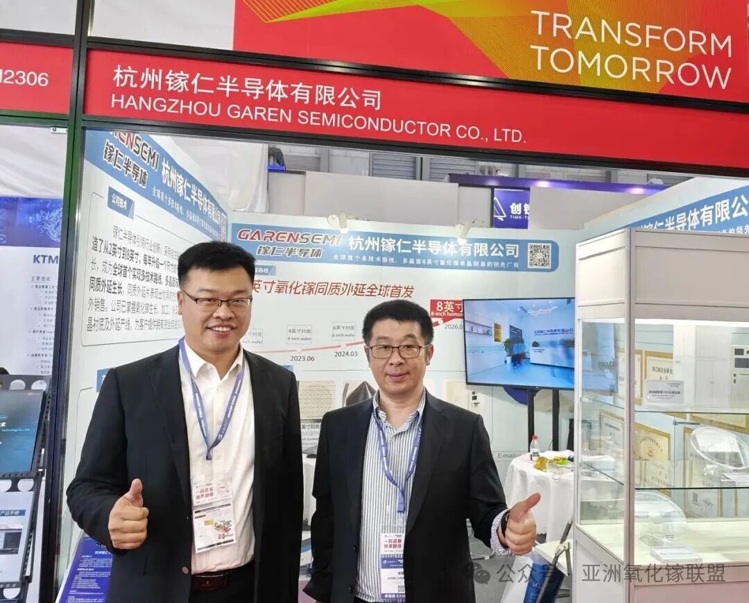
On March 25, 2026, SEMICON CHINA 2026—the world’s largest and most prestigious semiconductor industry event—officially opened at the Shanghai New International Expo Center. Hangzhou GAREN Semiconductor Co., Ltd. (hereinafter referred to as “GAREN SEMI”) made a high-profile appearance, showcasing its internationally debut 8-inch Gallium Oxide homoepitaxial wafer along with other key Gallium Oxide products. On the first day of the exhibition, GAREN SEMI’s booth was packed with visitors, drawing continuous attention and attracting significant interest from professionals across the global semiconductor industry.
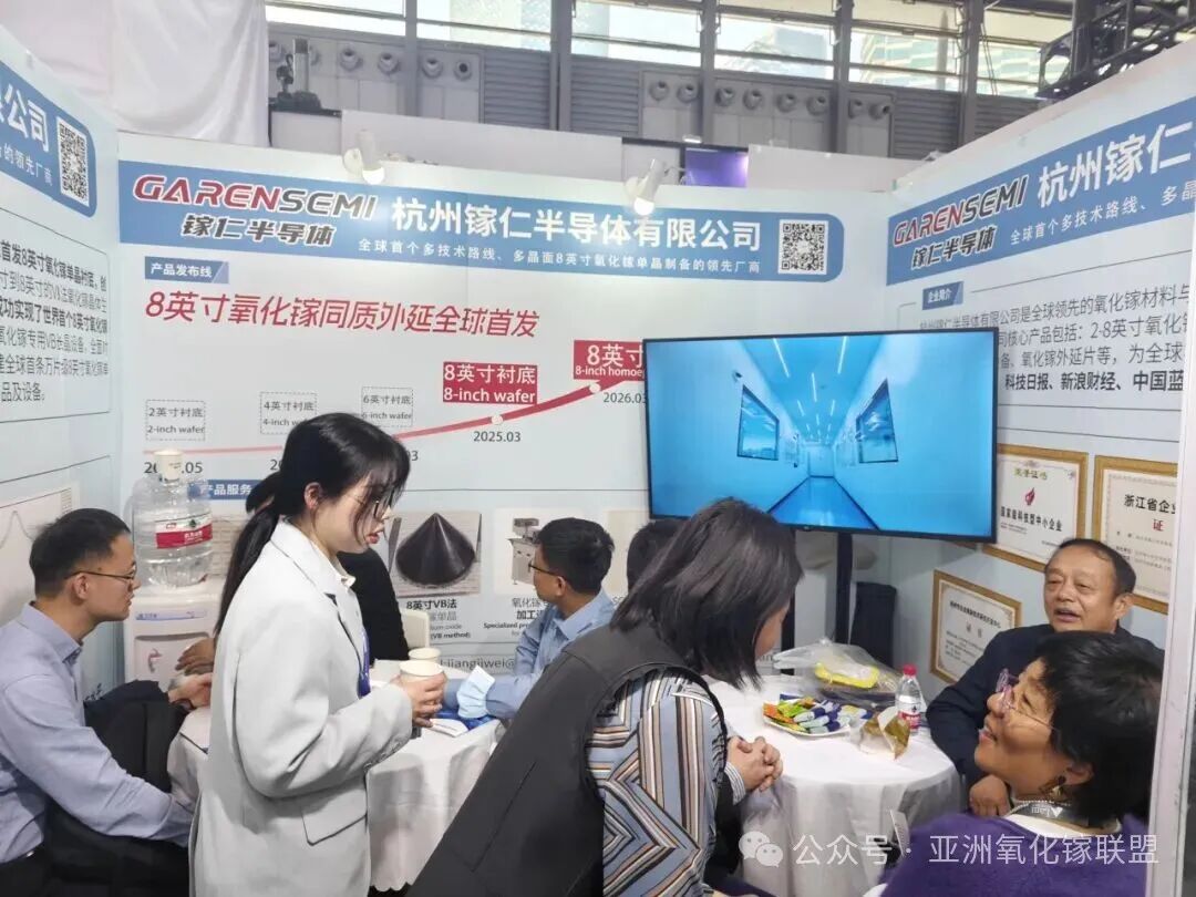
Figure 1: GAREN SEMI Booth at the Exhibition
As the world’s first leading company to achieve the preparation of 8-inch Gallium Oxide single crystals across multiple technological routes and crystal planes, Hangzhou GAREN Semiconductor (GAREN SEMI) focused its exhibition on showcasing the internationally debuted 8-inch Gallium Oxide homoepitaxial wafer, along with core products including 8-inch, 6-inch, 4-inch, and 2-inch Gallium Oxide substrates. The display comprehensively highlighted the company’s technological breakthroughs and innovations across the upstream Gallium Oxide industry chain.
Among them, the 8-inch Gallium Oxide homoepitaxial wafer, the star of the exhibition, has been authoritatively certified by the Shenzhen Pinghu Laboratory. With excellent quality and core performance at the international leading level, it fully addresses the long-standing industry challenge of achieving both large size and high quality simultaneously.
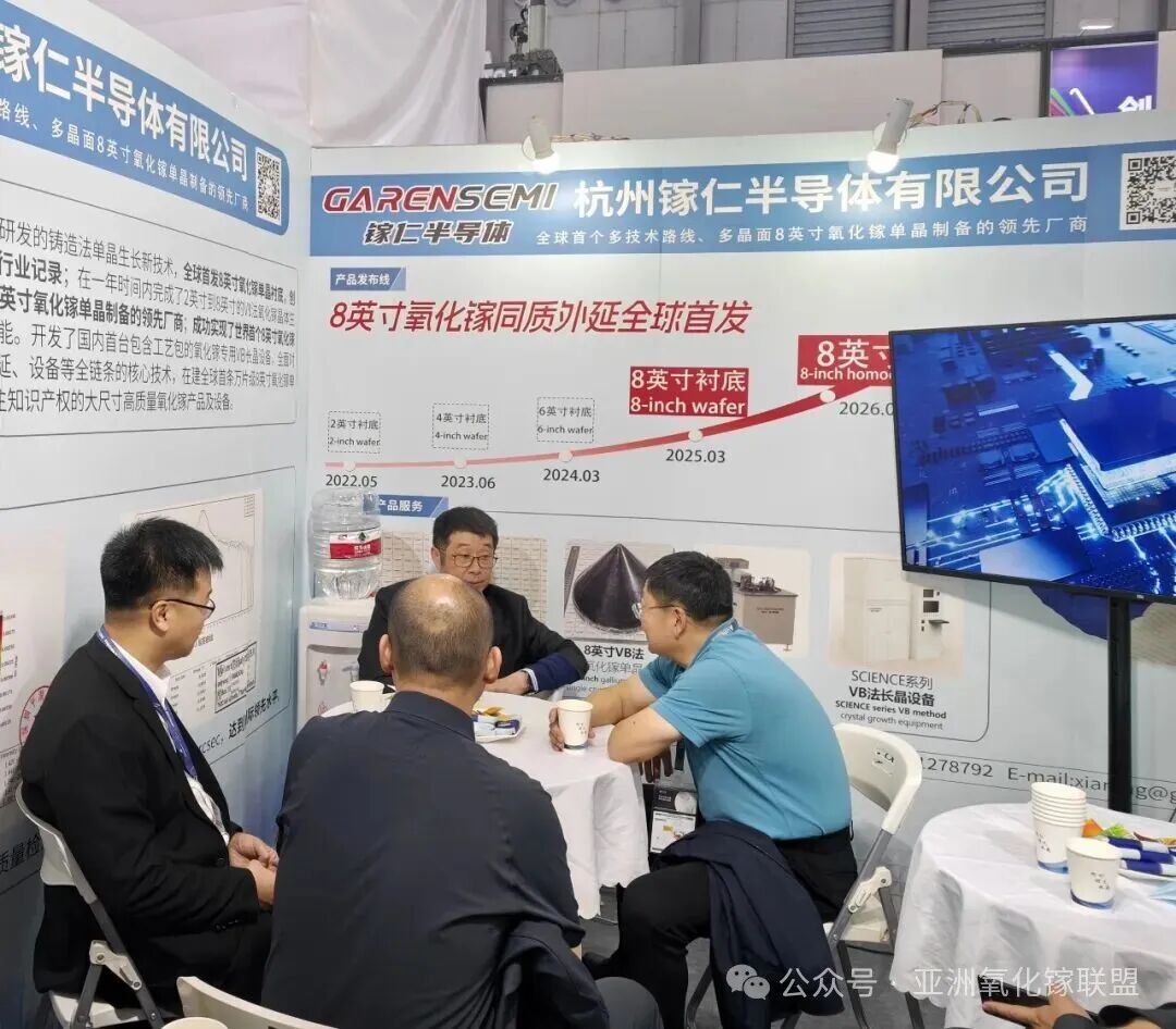
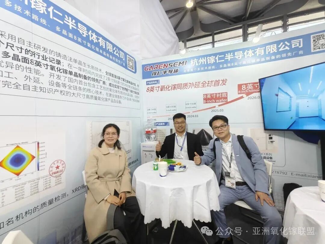
Figures 2 & 3: Industry Professionals Engaging at the GAREN SEMI Booth
At the exhibition, GAREN SEMI’s booth was bustling with activity. Researchers, downstream companies, and industry experts from the global semiconductor ecosystem stopped by to consult and engage in in-depth discussions, focusing on the performance parameters, fabrication processes, application scenarios, and potential for technological collaboration regarding the 8-inch Gallium Oxide homoepitaxial wafer.
This internationally debuted product, with its outstanding crystal quality, ultra-low defect density, and excellent electrical performance, quickly became the center of attention. It fully demonstrated GAREN SEMI’s global leadership in large-size Gallium Oxide homoepitaxy and underscored the core value of homoepitaxial growth as the optimal path for the industrialization of Gallium Oxide.
SEMICON CHINA 2026 provided not only a prime stage for GAREN SEMI to showcase its technological capabilities and product advantages but also a critical opportunity to connect with global industry resources and expand collaboration channels. The overwhelming turnout on the first day highlighted the industry’s keen attention to the development of wide-bandgap semiconductors and affirmed recognition of GAREN SEMI’s technical strength and growth potential.
Looking ahead, Hangzhou GAREN Semiconductor will continue to uphold its commitment to technological innovation, deeply cultivate the upstream Gallium Oxide industry chain, and continuously overcome core technological bottlenecks while enhancing its product portfolio. By delivering higher-quality products and services, the company aims to repay the industry’s trust and seize the lead in the global wide-bandgap semiconductor sector.
We warmly welcome industry peers to visit GAREN SEMI at SEMICON CHINA 2026 (Hall N2, Booth 2308) to explore emerging industry trends together and jointly shape the future of the semiconductor industry!
About GAREN SEMI
Hangzhou Garen Semiconductor Co., Ltd. is a world-leading provider of Gallium Oxide materials and equipment solutions, focusing on R&D and industrialization in the ultra-wide bandgap semiconductor field. The company’s core products include 2–8-inch Gallium Oxide single crystals and substrates (with 8-inch being the world’s first), Gallium Oxide Vertical Bridgman (VB) crystal growth equipment, Gallium Oxide epitaxial wafers, etc. It is committed to building a full-chain product system of “equipment–crystal–substrate–epitaxy” to provide systematic solutions for global customers. The company’s achievements in Gallium Oxide have been specially reported by well-known media including People’s Daily, Xinhua News Agency, Science and Technology Daily, Sina Finance, China Blue News, and The Paper.
Enterprise Honors Summary
Recognized as a National-level Science and Technology Small and Medium-sized Enterprise and Zhejiang Innovative Small and Medium-sized Enterprise in 2023;Awarded Zhejiang Specialized, Sophisticated, Unique and New Small and Medium-sized Enterprise in 2024;Approved as a High-tech Enterprise in 2025;Won the SEMI Outstanding Contribution Award for Sustainable Development at SEMICON CHINA 2025, the Together Progress Award at the Jufeng Summit Forum (JFSC) and Compound Semiconductor Industry Expo, the Innovation Vitality Award of Zhejiang Semiconductor Industry, the Second Prize in the Enterprise Group of the 10th “Maker China” Zhejiang Provincial Finals, the Top 500 Enterprise Group of the 10th “Maker China” SME Innovation and Entrepreneurship Competition, and the 2024–2025 Semiconductor Material Industry Contribution Award;The major breakthrough in the preparation of 8-inch Gallium Oxide single crystals and substrates was selected as one of the “Top 10 Advances in China’s Third-Generation Semiconductor Technology 2025” and “Major Scientific and Technological Achievements 2025” by the Department of Science and Technology of Zhejiang Province;Led the formulation of 2 group standard drafts, participated in drafting 1 national standard, and participated in promoting 1 group standard draft in the Gallium Oxide field;Supported by the “5213” Excellence Program of Xiaoshan District, Hangzhou, Zhejiang Province, and approved to establish Zhejiang Enterprise Research Institute;Obtained the quality management system certification;Granted 14 authorized invention patents at home and abroad (including patents in the US, Japan and other countries), with more than 50 patents pending.
For more information about Garen Semiconductor and its products, please visit our official website: http://garen.cc/
Or contact us via the following ways:
Mr. Jiang: 15918719807
E-mail: jiangjiwei@garen.cc
Mr. Xia: 19011278792
E-mail: xianing@garen.cc
