Paper Sharing
【Domestic Papers】Recent advances in heterojunction engineering of β-Ga₂O₃-based solar-blind ultraviolet photodetectors
日期:2026-03-26阅读:228
Researchers from the Shanghai Dianji University have published a dissertation titled " Recent advances in heterojunction engineering of β-Ga2O3-based solar-blind ultraviolet photodetectors " in Semiconductor Science and Technology.
Background
The rapid advancement of information technologies, including artificial intelligence, big data, cloud computing, and 5G communications, has escalated performance requirements for electronic informa tion systems. As fundamental components of optoelectronic technology, photodetectors play indispens able roles in this domain and have emerged as a global research priority. Beyond the solar-blind ultraviolet (SBUV) regime, photodetectors operating across the visible, infrared, and terahertz spectra are also critically enabling the ongoing evolution of high-speed communication systems, including 5G and the emerging 6G networks. Devices operating in these complementary spectral windows facilitate high-bandwidth data transmission, environmental sensing, biomedical diagnostics, and secure commu nications, collectively supporting the infrastructure of the internet of things (IoTs) and intelligent sensing networks. Within this broad photodetector landscape, solar-blind UV photodetectors occupy a unique spectral niche.
Abstract
In recent years, the demand for high-performance photodetectors in environmental monitoring, specialized detection, and space communications has grown significantly. Solar-blind ultraviolet (SBUV) photodetectors have become a research hotspot due to their unique spectral selectivity and high sensitivity. As an ultra-wide bandgap semiconductor material (∼ 4.9 eV), β-Ga2O3 is regarded as a highly promising material for SBUV detection owing to its excellent intrinsic properties, including high breakdown field strength, outstanding thermal stability, and superior response in the SBUV band. Research demonstrates that constructing β-Ga2O3-based heterojunctions effect ively regulates interfacial band structures, significantly enhances photogenerated carrier separation efficiency, improves device responsivity while suppressing dark current, and offers potential path ways to address performance limitations of conventional photodetectors. Based on a coordinated material-device optimization framework, this review systematically summarizes recent research advances in β-Ga2O3 heterojunction SBUV photodetectors, with a focus on performance optim ization strategies from three dimensions: material property modulation, heterojunction interface engineering, and device structure design. Future development directions are also discussed.
Conclusion
Looking forward, the development of β-Ga2O3 heterojunction photodetectors will advance along three primary trajectories. In materials research, deepening the understanding of doping mechanisms to discover viable p-type doping solutions and exploring novel material combinations with β-Ga2O3 is likely to be essential; multitechnology integration approaches should optimize heterointerface qual ity and band structure to enhance device performance. For device design and fabrication, continu ous innovation in architectures—including novel heterojunction configurations, nanostructuring, and micro/nanofabrication—is expected to drive miniaturization, integration, and functional intelligence, while refined growth techniques must improve film quality, production uniformity, and cost efficiency. Regarding application expansion, emerging technologies like 5G communications and IoT will enable broader deployment of β-Ga2O3 photodetectors in high-speed optical networks, environmental monit oring systems, and wearable electronics. Furthermore, the integration of β-Ga2O3 photodetectors with other on-chip photonic components is emerging as a key direction. Recent demonstrations, such as MOCVD-grown Ga2O3 optical waveguides on silicon substrates, pave the way for compact, mono lithic SBUV photonic systems that combine detection, modulation, and routing functionalities. Beyond hardware integration, the further convergence of these devices with artificial intelligence and big data analytics will empower intelligent sensing, real-time diagnostics, and autonomous decision-making within broader networks. Through sustained resolution of technical bottlenecks, β-Ga2O3 heterojunc tion photodetectors are poised to play increasingly vital roles in optoelectronics, accelerating industrial advancement across multiple sectors.
Project Support
This work was financially supported by the National Natural Science Foundation of China (Grant No. U22A2073).
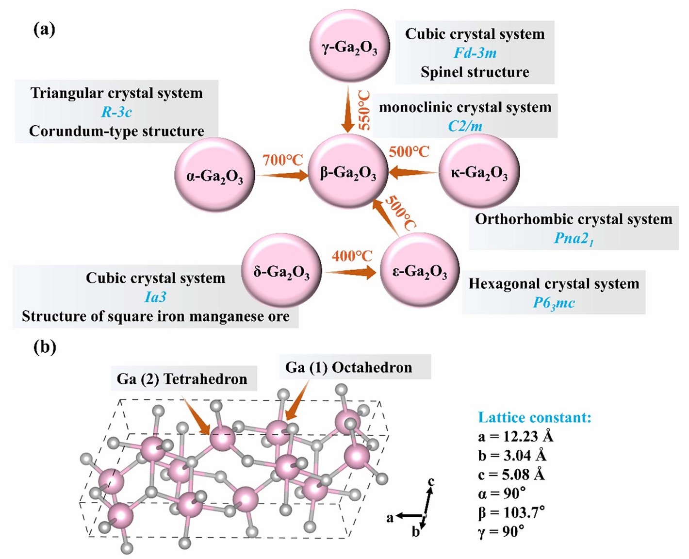
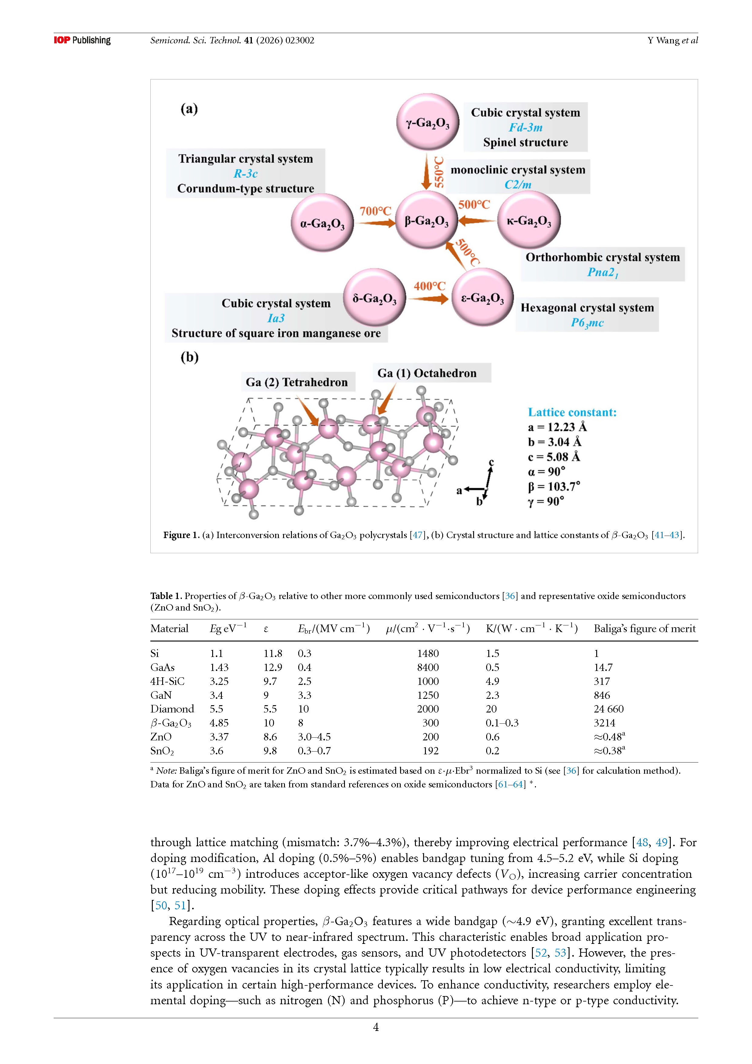
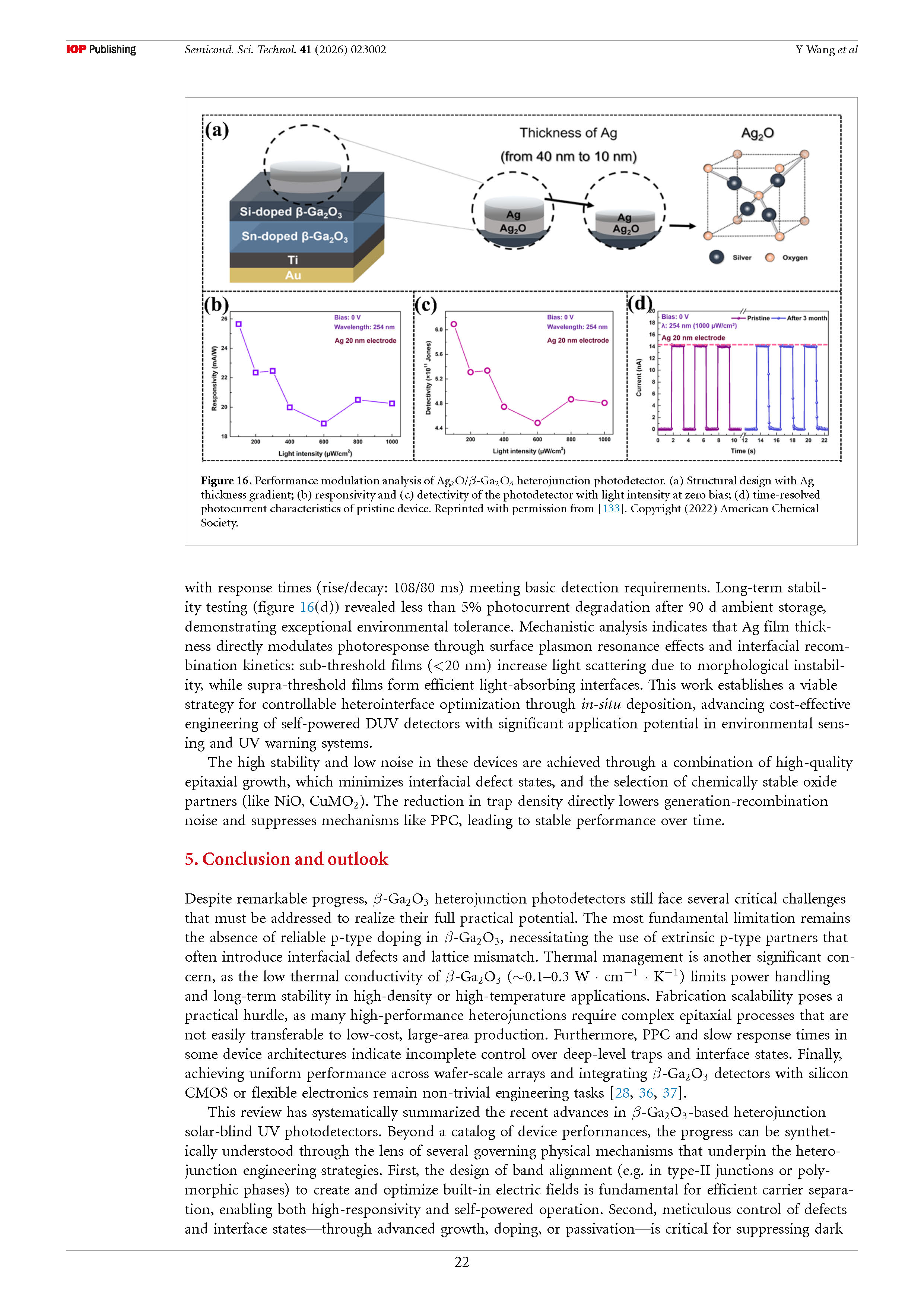
Figure1.(a)Interconversion relations of Ga2O3 polycrystals (b) Crystal structure and lattice constants of β-Ga2O3
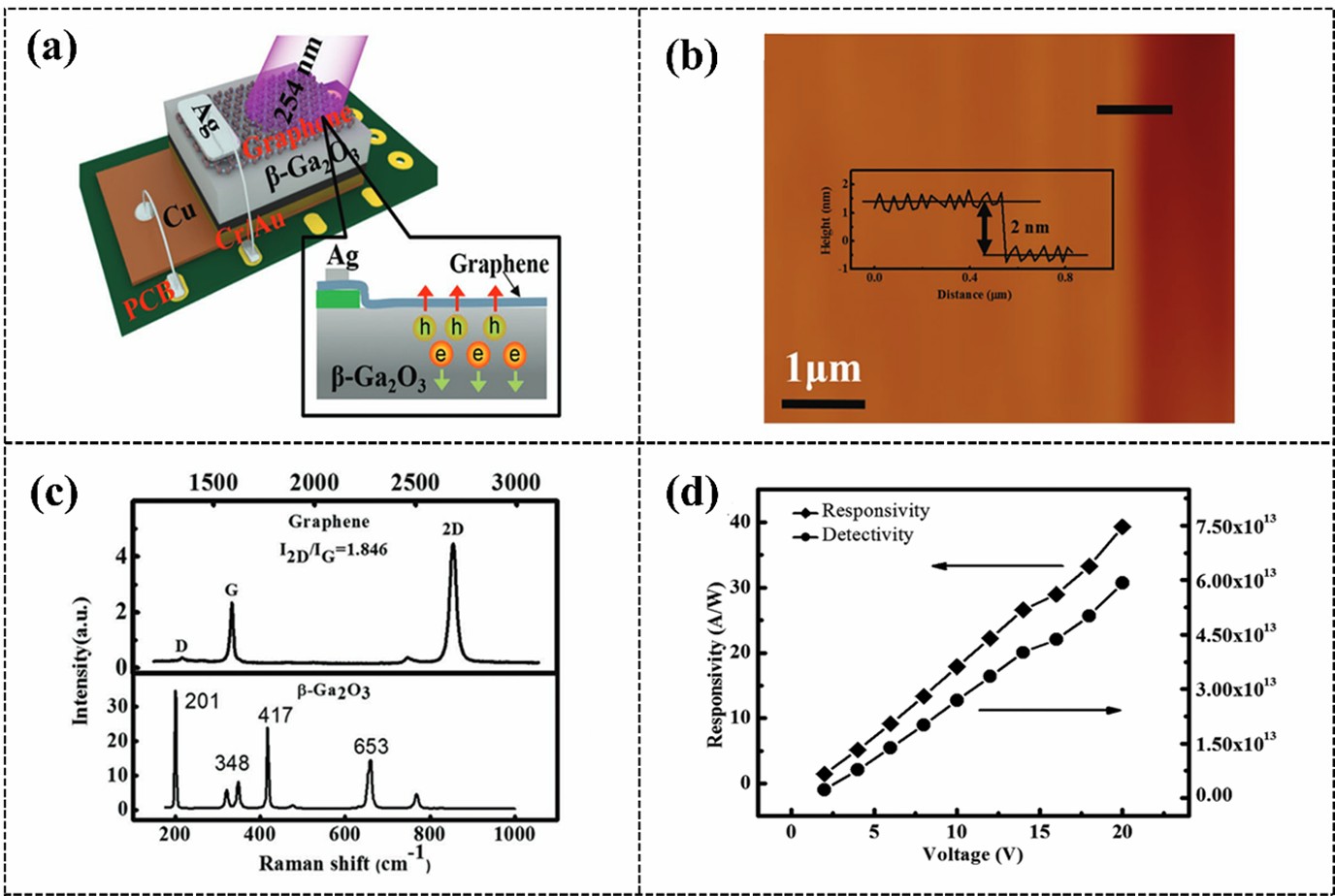
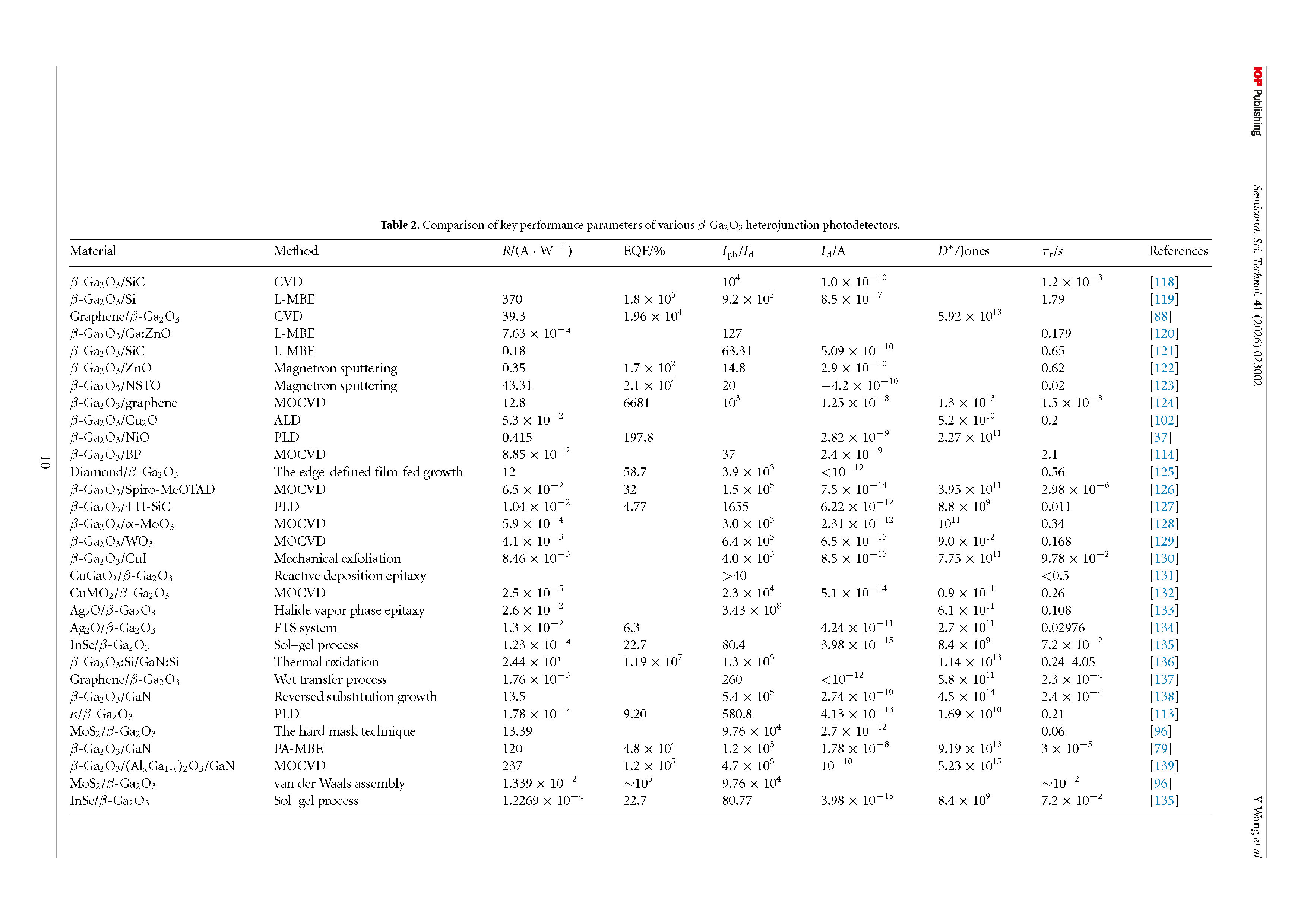
Figure 2. Structural and optoelectronic analysis of MLG/β-Ga2O3 heterojunction deep-ultraviolet photodetector. (a) Schematic of the device architecture; (b) AFM topography of MLG film on β-Ga2O3 substrate; (c) comparative Raman spectra of MLG and β-Ga2O3; (d) voltage-dependent evolution of responsivity and detectivity.
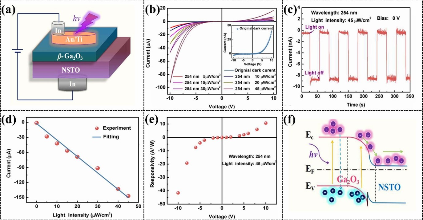
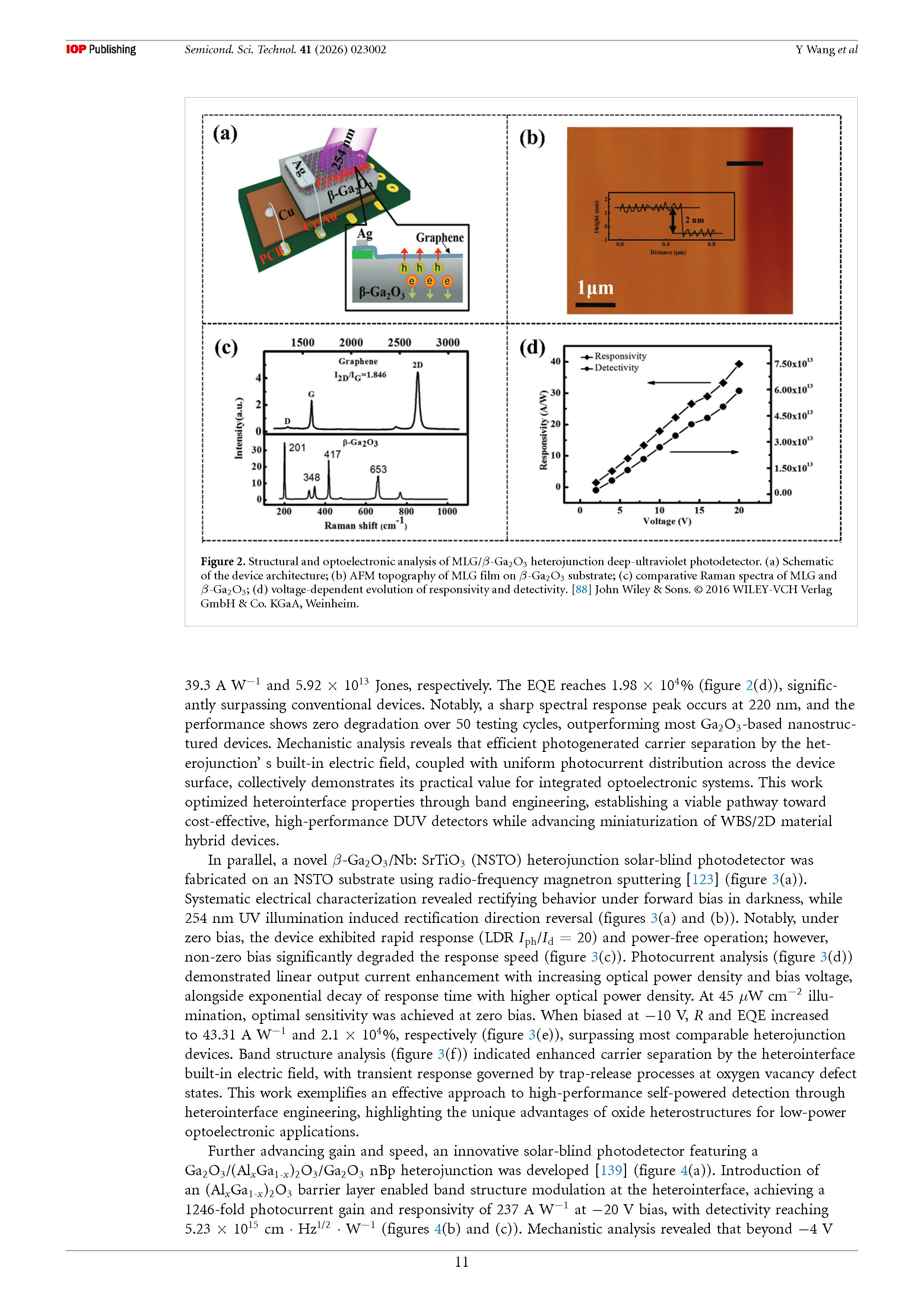
Figure 3. Structural and optoelectronic characterization of β-Ga2O3/NSTO heterojunction photodetector. (a) Schematic diagram of the device architecture; (b) Current–voltage (I–V) characteristics under dark condition and 254 nm illumination with varying light intensities (inset: enlarged view of dark I–V curve); (c) Photoresponse switching behavior at 0 V bias under 45 µW cm−2 254 nmillumination; (d) Time-resolved photocurrent as a function of incident light intensity; (e) Voltage-dependent responsivity evolution; (f) Energy band alignment diagram illustrating interfacial carrier dynamics.
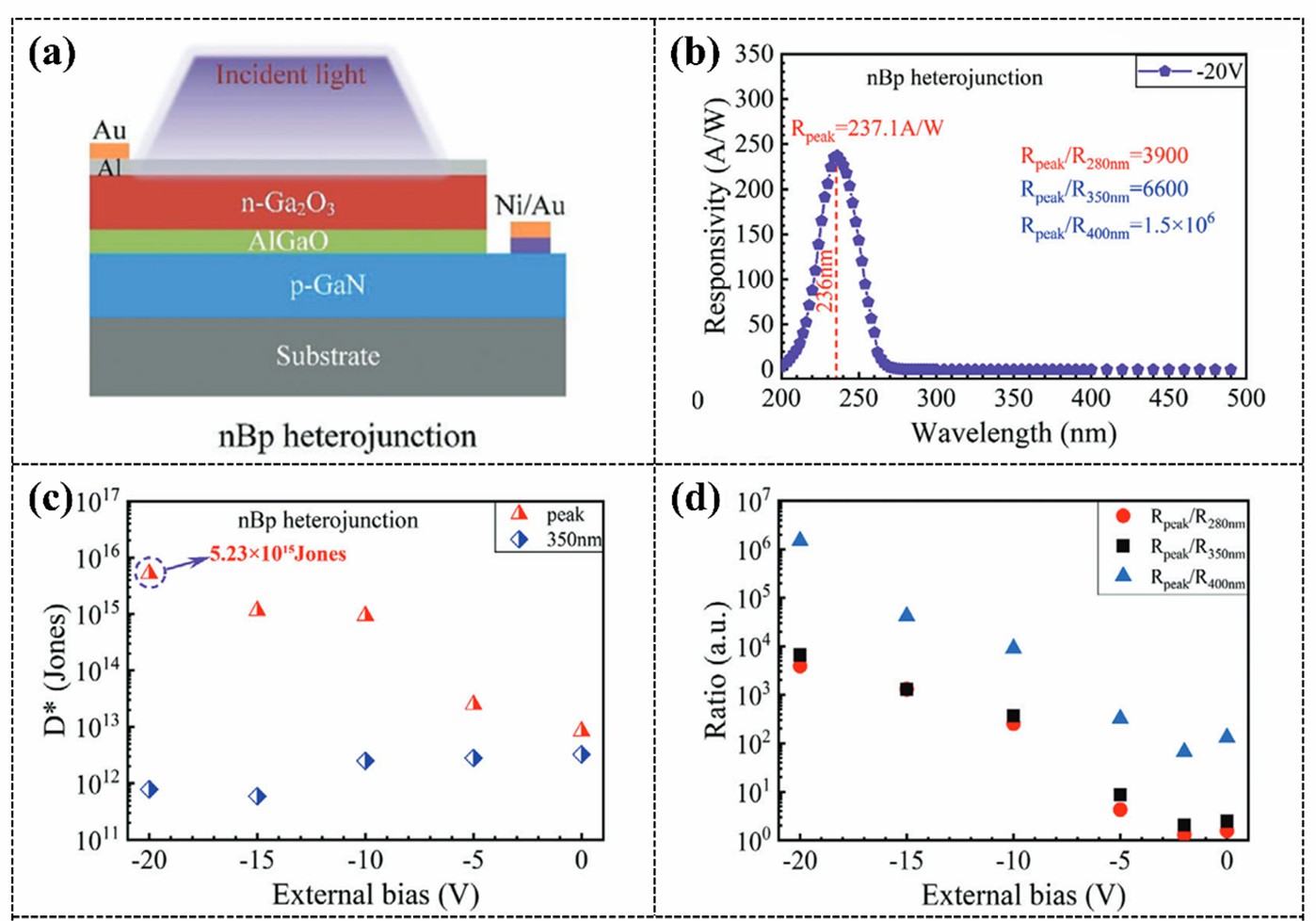
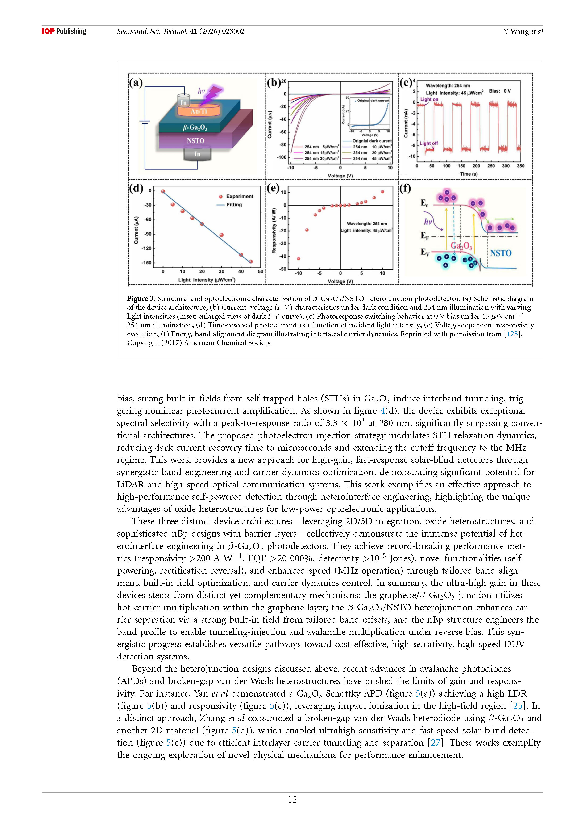
Figure4.Multidimensional performance modulation of nBp heterojunction photodetector. (a)Schematic diagram of nBp heterojunction; (b)Photoresponse characterization of the nBp heterojunction device: Under−20Vbias; (c)D∗ of the nBp photodetector under reverse voltage; (d)Relationship between the ratio of peak responsivity to the responsivity at different wavelengths under different bias voltages.
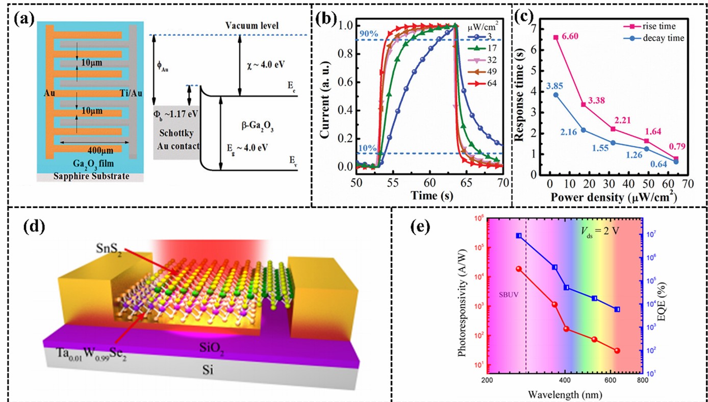
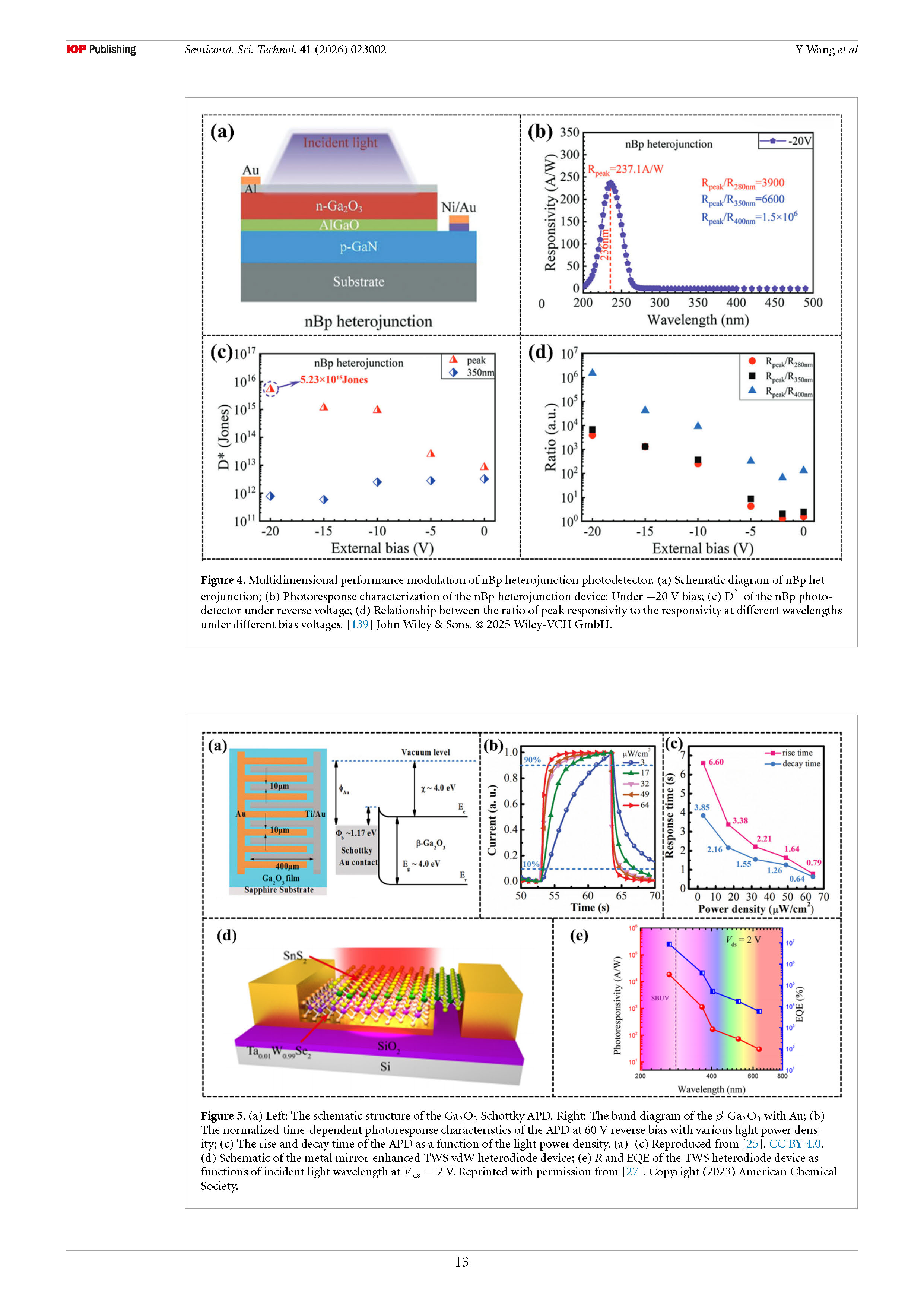
Figure5.(a)Left:The schematic structure of the Ga2O3 Schottky APD. Right: The band diagram of the β-Ga2O3 with Au; (b) The normalized time-dependent photoresponse characteristics of the APD at 60V reverse bias with various light power density; (c) The rise and decay time of the APD as a function of the light power density. (d)Schematic of the metal mirror-enhanced TWS vdW heterodiode device; (e)R and EQE of the TWS heterodiode device as functions of incident light wavelength at Vds = 2V.
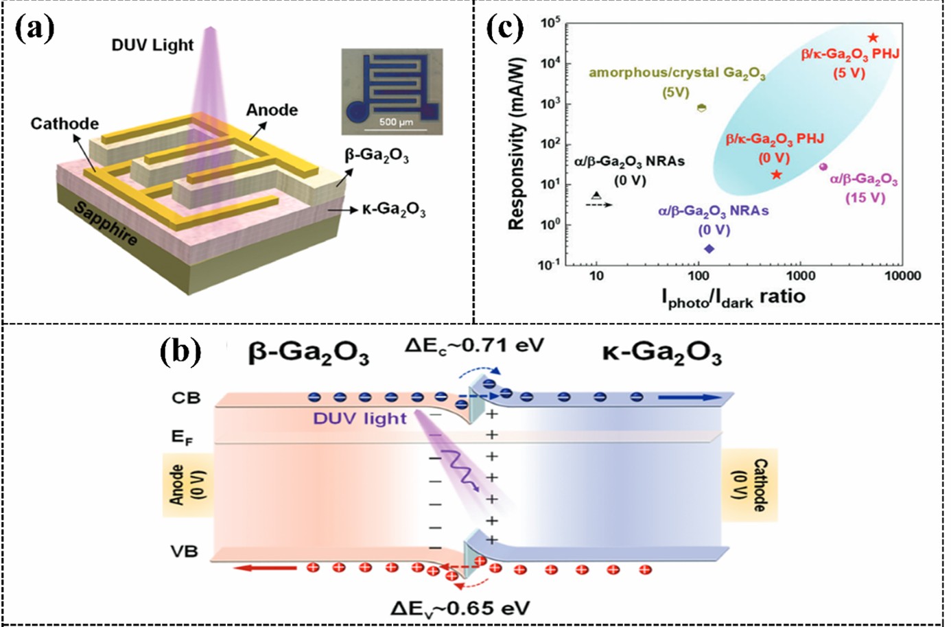
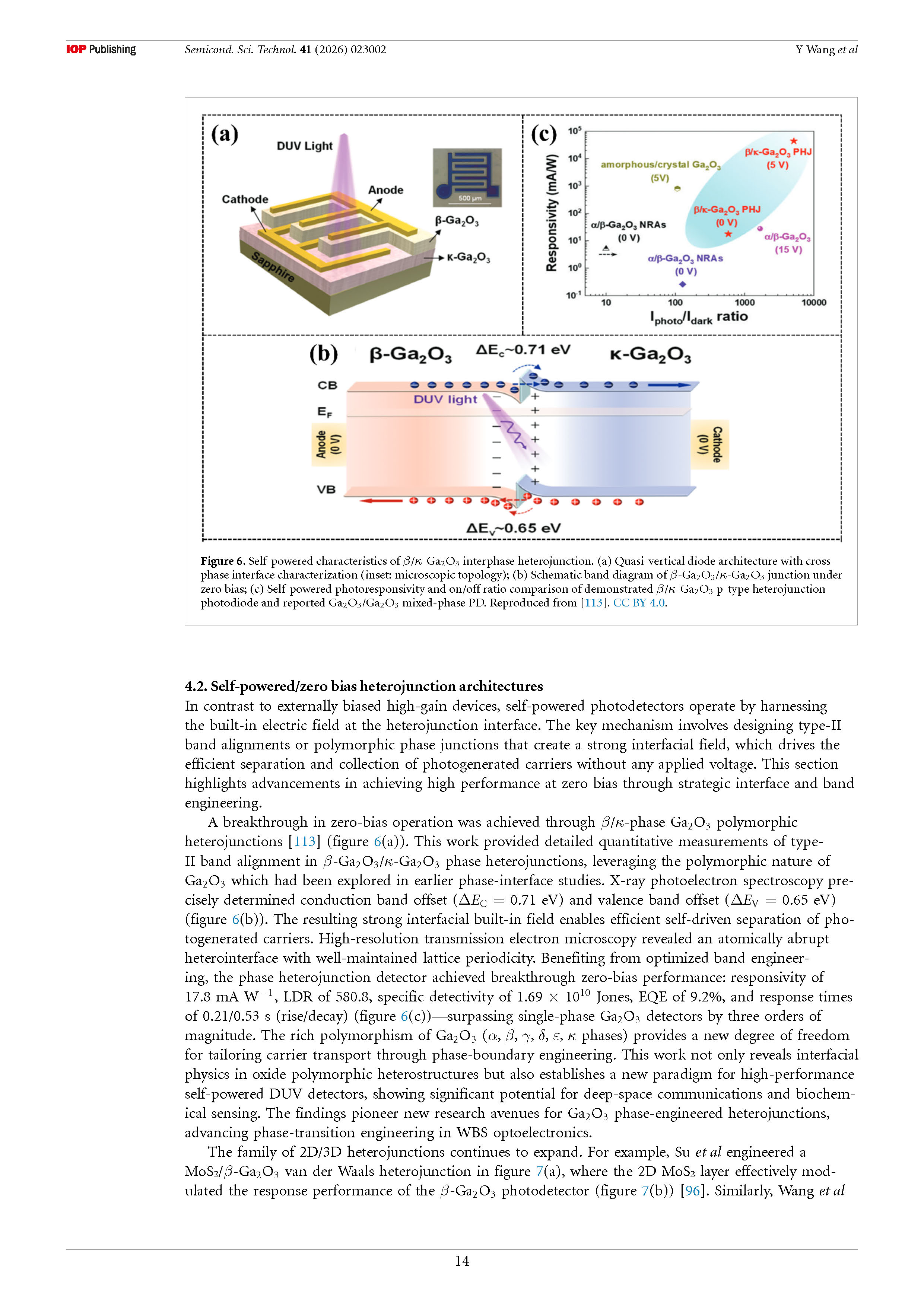
Figure 6. Self-powered characteristics of β/κ-Ga2O3 interphase heterojunction. (a) Quasi-vertical diode architecture with cross phase interface characterization (inset: microscopic topology); (b) Schematic band diagram of β-Ga2O3/κ-Ga2O3 junction under zero bias; (c) Self-powered photoresponsivity and on/off ratio comparison of demonstrated β/κ-Ga2O3 p-type heterojunction photodiode and reported Ga2O3/Ga2O3 mixed-phase PD.
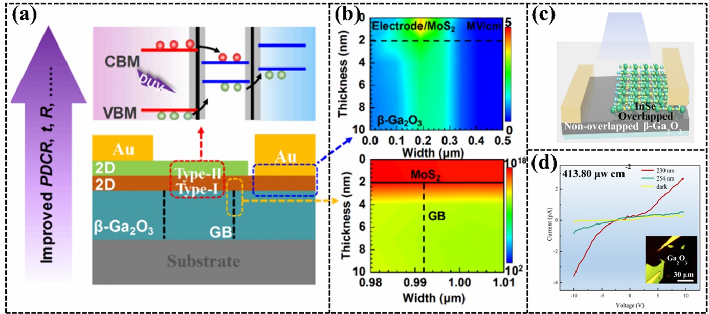
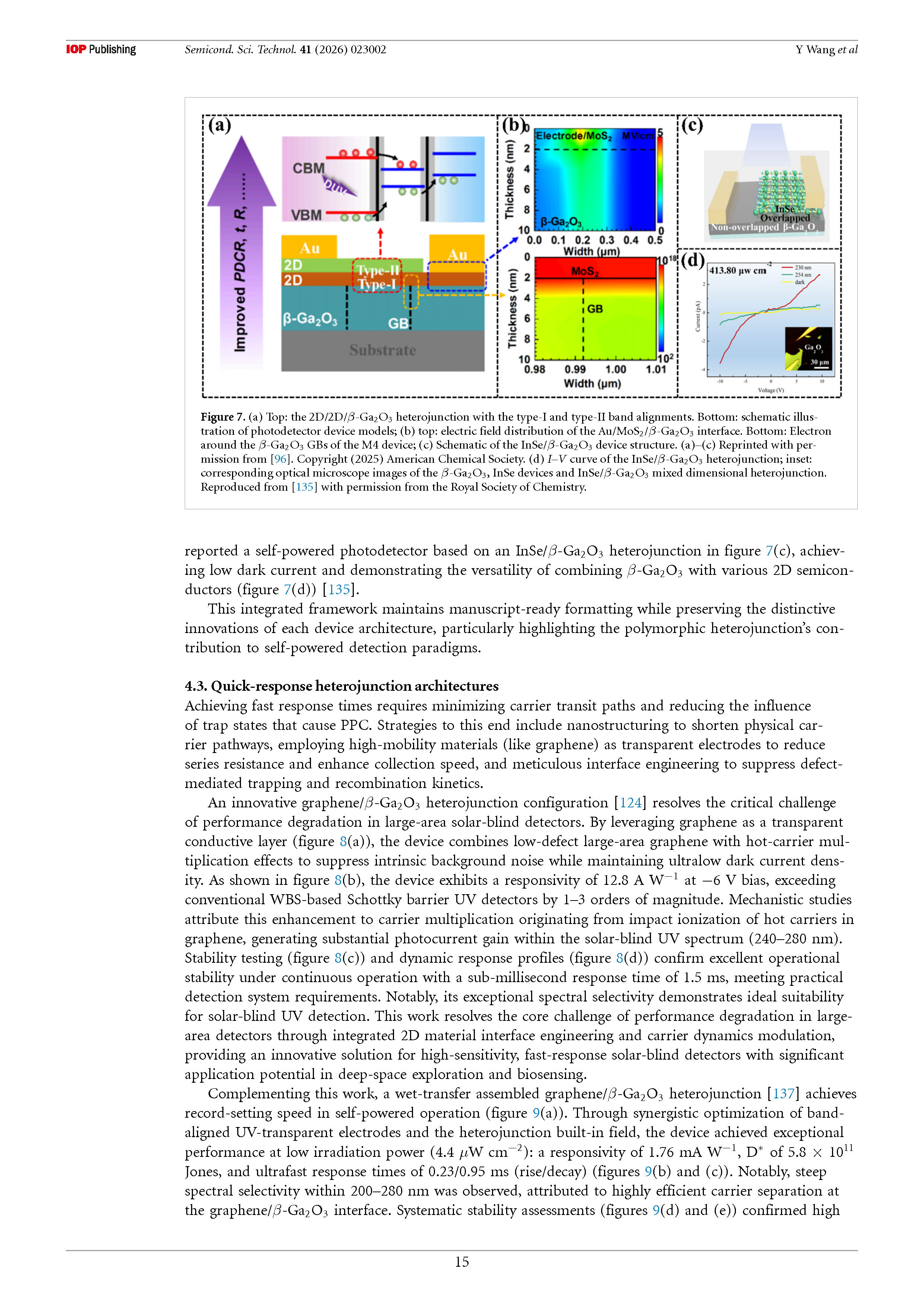
Figure 7. (a) Top: the 2D/2D/β-Ga2O3 heterojunction with the type-I and type-II band alignments. Bottom: schematic illus tration of photodetector device models; (b) top: electric field distribution of the Au/MoS2/β-Ga2O3 interface. Bottom: Electron around the β-Ga2O3 GBs of the M4 device; (c) Schematic of the InSe/β-Ga2O3 device structure.(d) I–V curve of the InSe/β-Ga2O3 heterojunction; inset: corresponding optical microscope images of the β-Ga2O3, InSe devices and InSe/β-Ga2O3 mixed dimensional heterojunction.
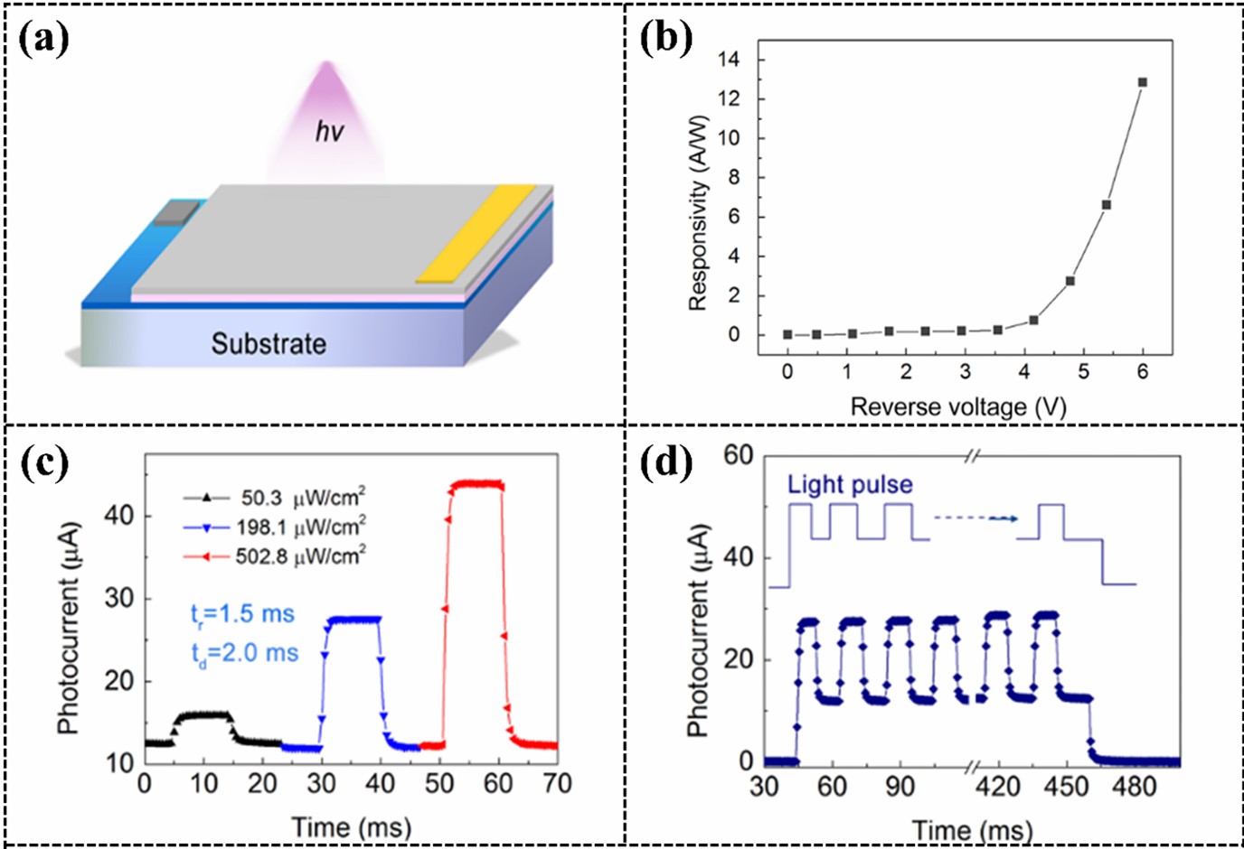
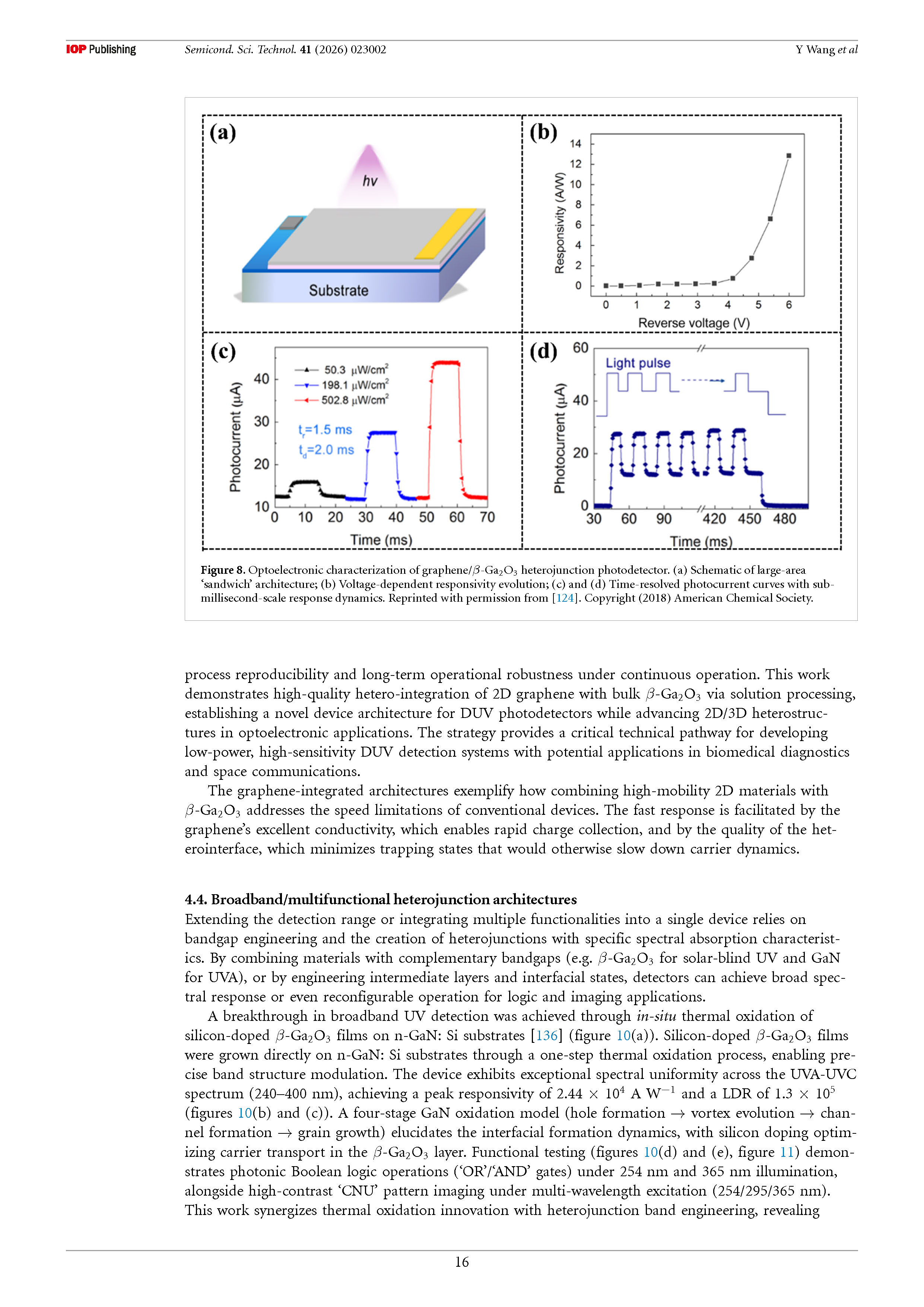
Figure 8. Optoelectronic characterization of graphene/β-Ga2O3 heterojunction photodetector. (a) Schematic of large-area ‘sandwich’ architecture; (b) Voltage-dependent responsivity evolution; (c) and (d) Time-resolved photocurrent curves with sub millisecond-scale response dynamics.
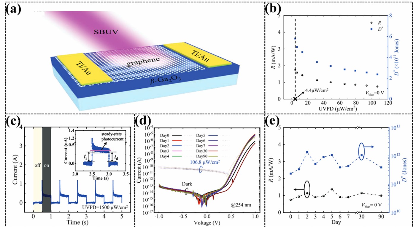
Figure9.Self-powered characteristics of graphene/β-Ga2O3heterojunction photodetector. (a)Schematic diagram of 3D heterogeneous structure; (b)Optical-power-dependent responsivity and specific detectivity; (c)Time response with on-off cycles at the bias voltage of 0V. Inset: enlarged view of a single cycle; (d) Stability of the photo detector, long-time exposure under atmospheric environment; (e) Bias-free photo conversion efficiency optimization.
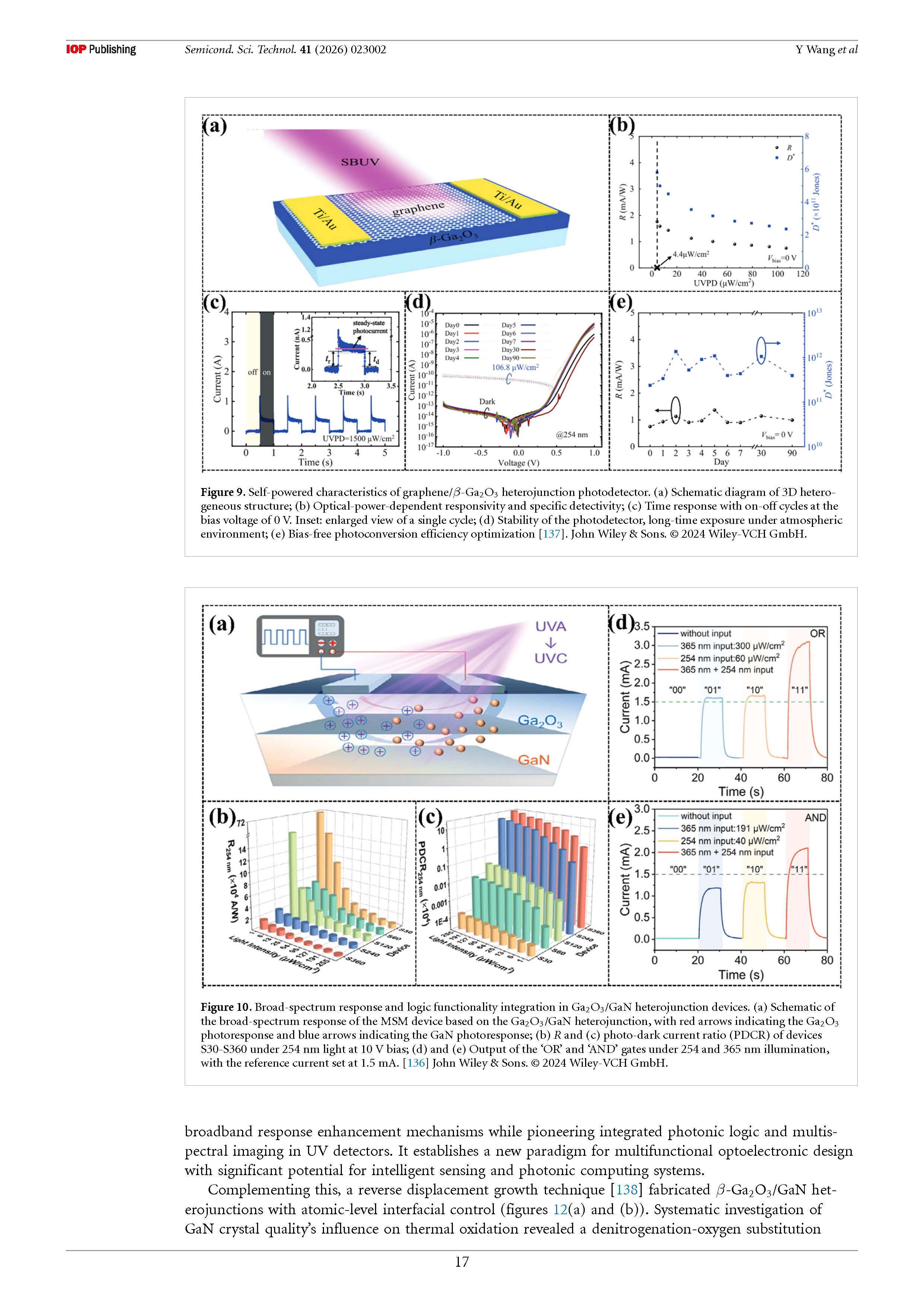
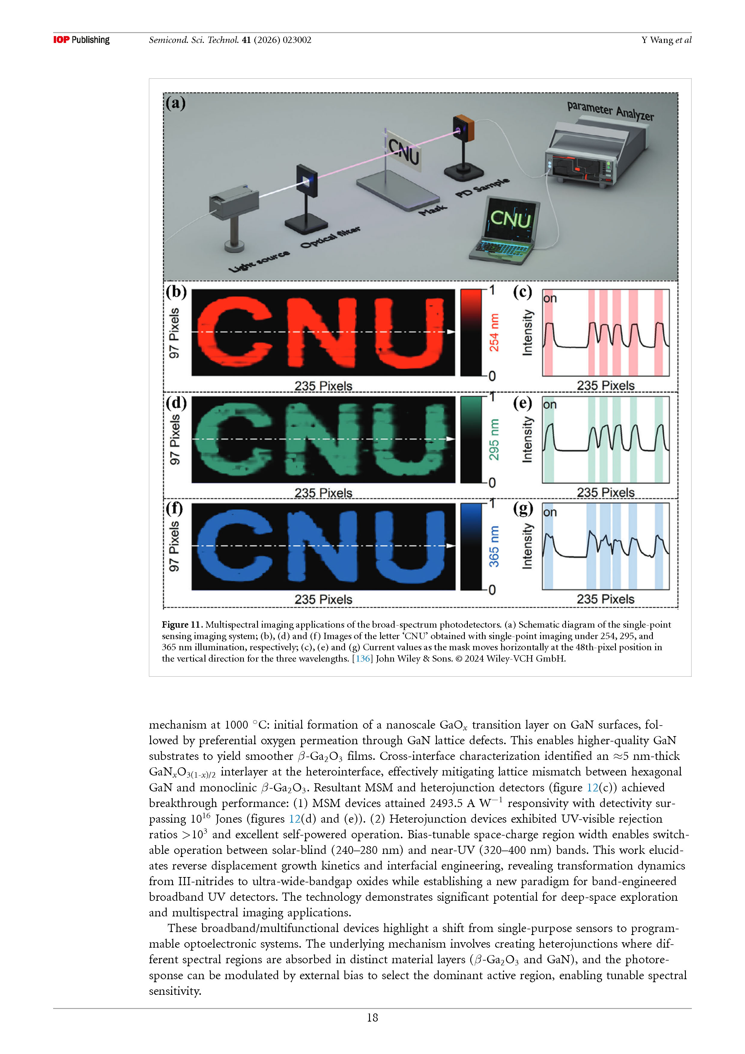
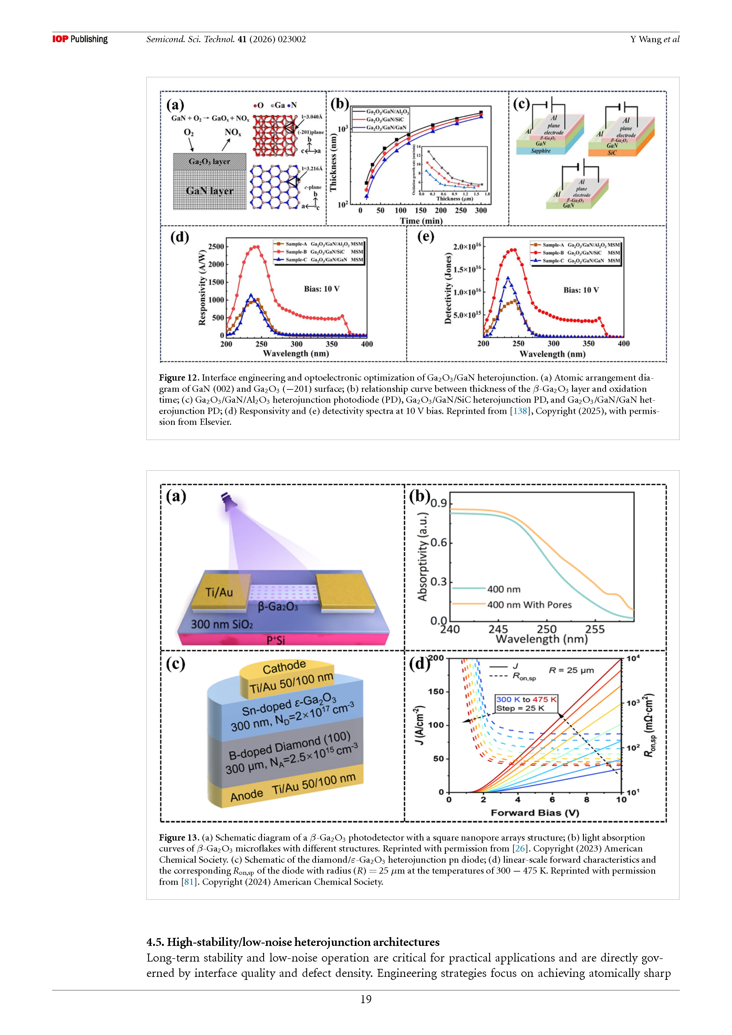
Figure10.Broad-pectrum response and logic functionality integration in Ga2O3/GaN heterojunction devices. (a)Schematic of the broad-spectrum response of the MSM device based on the Ga2O3/GaN heterojunction, with red arrows indicating the Ga2O3 photo response and blue arrows indicating the GaN photo response; (b)Rand (c)photo-dark current ratio (PDCR) of devices S30-S360 under 254 nm light at 10V bias; (d) and (e) Out put of the ‘OR’ and ‘AND’ gates under 254 and 365 nm illumination, with the reference current set at 1.5mA.
DOI:
doi.org/10.1088/1361-6641/ae4263