Paper Sharing
【Member Papers】Self-catalytic growth and ultraviolet detection performance of Cu: β-Ga₂O₃ nanowires
日期:2026-03-26阅读:192
Researchers from the Liaoning Normal University and Dalian University of Technology have published a dissertation titled "Self-catalytic growth and ultraviolet detection performance of Cu: β-Ga2O3 nanowires" in Physica B: Condensed Matter.
Background
β-Ga2O3 is a semiconductor material with an ultrawide bandgap width of about 4.9 eV, and its cut-off wavelength is located at 254 nm, precisely within the solar-blind ultraviolet range of 220-280 nm. Futhermore, β-Ga2O3 possesses many inherent advantages, including a high breakdown electrical field (∼8 MV/cm), robust chemical and thermal stability, and high radiation hardness. These outstanding properties make β-Ga2O3 an excellent candidate for manufacturing solar-blind UV photodetectors. Currently, some solar-blind UV detectors based on β-Ga2O3 bulk single crystals, thin films, and micro/nano structures have been reported. Due to their high crystal quality and surface effect, one-dimensional nanowire-based photodetectors demonstrated superior photoelectric performance compared to traditional thin film-based devices. Currently, the preparation of one-dimensional β-Ga2O3 nanomaterials mostly requires depositing a layer of metal catalyst (such as Au) on the substrate. The additional metal catalyst not only increases costs but also leads to resource waste. Self-catalytic VLS growth is a favorable method for fabricating nanomaterials, where metal elements from the source material serve as catalysts for the growth process. At present, there are very few literatures on the self-catalytic VLS mechanism for preparation of β-Ga2O3 nanomaterials, and only reports using Ga seeds have been available. Park et al. prepared β-Ga2O3 nanowires via radio-frequency magnetron sputtering (RF-MS) deposition equipment with a powder target.
Abstract
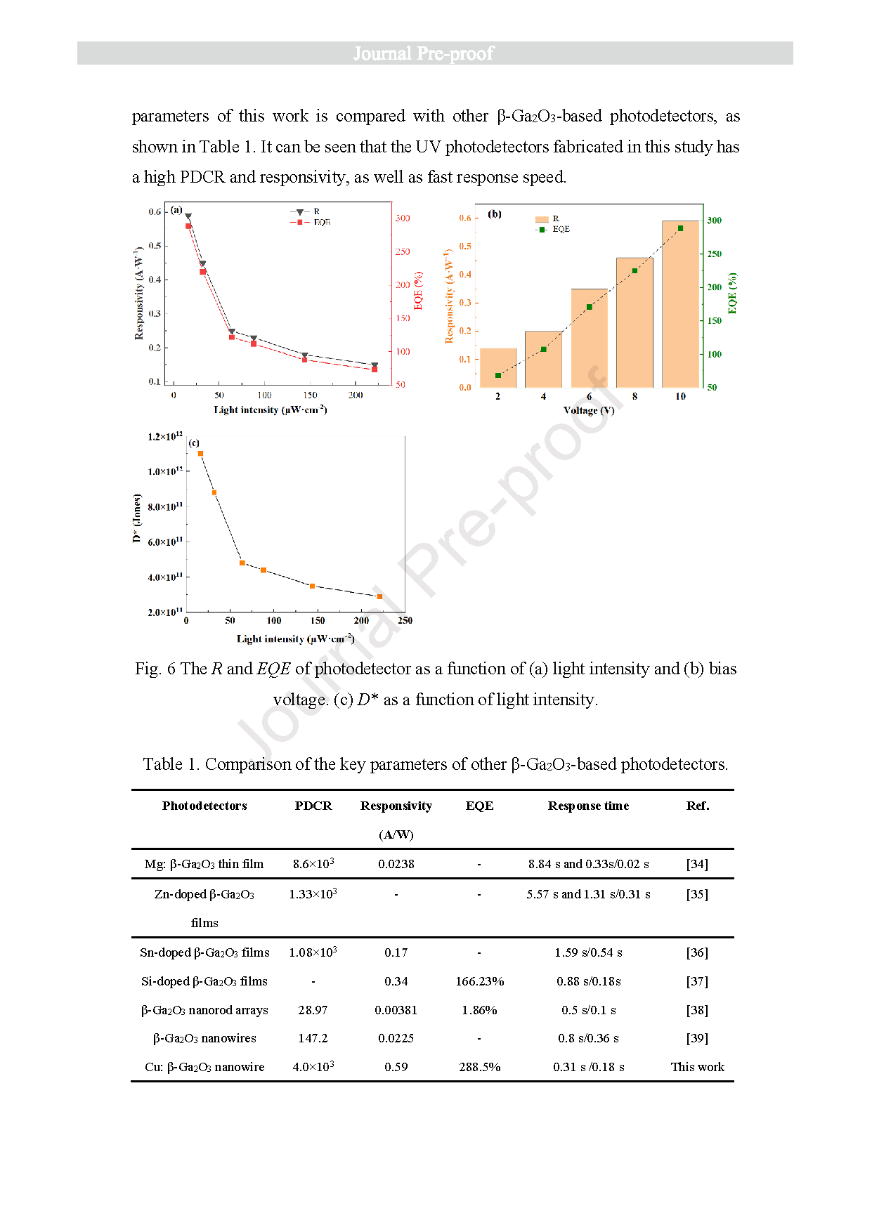
The growth of high-density Cu: β-Ga2O3 nanowires was achieved by chemical vapor deposition (CVD) based on a self-catalytic vapor-liquid-solid (VLS) process with self-assembled Cu seeds. The length of the nanowires up to 40 μm-60 μm, and the diameter is approximately 300-500 nm. Furthermore, the Cu: β-Ga2O3 nanowires were used to fabricate a photoconductive ultraviolet photodetector with indium-tin-oxide (ITO) electrodes. The PDCR of the photodetector reached 4.0 × 10³ at 10 V bias under 254 nm. The device also exhibited fast response characteristics, with a rise time of 0.31 s and a fall time of 0.18 s. The Cu: β-Ga2O3 nanowires photodetector exhibit a high responsivity of 0.59 A/W, and a specific detectivity (D∗) of 1.1 × 10¹² Jones under 254 nm light with a light power density of 16 μW/cm2. This technique provides a simple and feasible method for the growth of self-catalytic β-Ga2O3 nanostructures.
Highlights
High-density Cu: β-Ga2O3 nanowires were fabricated through the self-catalytic VLS mechanism with self-assembled Cu seeds.
The Cu: β-Ga2O3 nanowires were used to fabricate photoconductive UV photodetector with ITO electrodes.
The responsivity and specific detectivity were calculated to be 0.59 A/W and 1.1 × 10¹² Jones.
Conclusions
Large-area and high-density Cu: β-Ga2O3 nanowires were grown by CVD method via self-catalytic VLS growth of self-assembled Cu seeds. The optical bandgap of Cu: β-Ga2O3 nanowires was estimated to 4.85 eV. A MSM photoconductive detector was fabricated by using grown Cu-doped β-Ga2O3 nanowires. Under 254 nm at 10 V, the PDCR of Cu: β-Ga2O3 nanowires devices reached as high as 4.0 × 10³. The response time was extremely rapid, with τr of 0.31 s and τd of 0.18 s. The higher PDCR, responsivity, specific detectivity and external quantum efficiency indicate that the Cu: β-Ga2O3 nanowires grown by self-catalytic VLS method possess excellent UV detection performance. This research provides valuable references for the growth of β-Ga2O3 nanostructures and their ultraviolet photodetection performance.
Project Support
This work is supported by the National Natural Science Foundation of China (No. 12075045), Dalian Science and Technology Innovation Fund Project (No. 2023JJ12GX016).
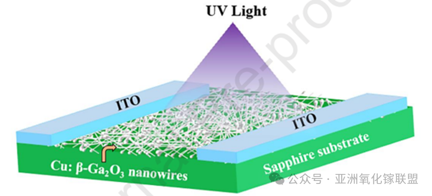
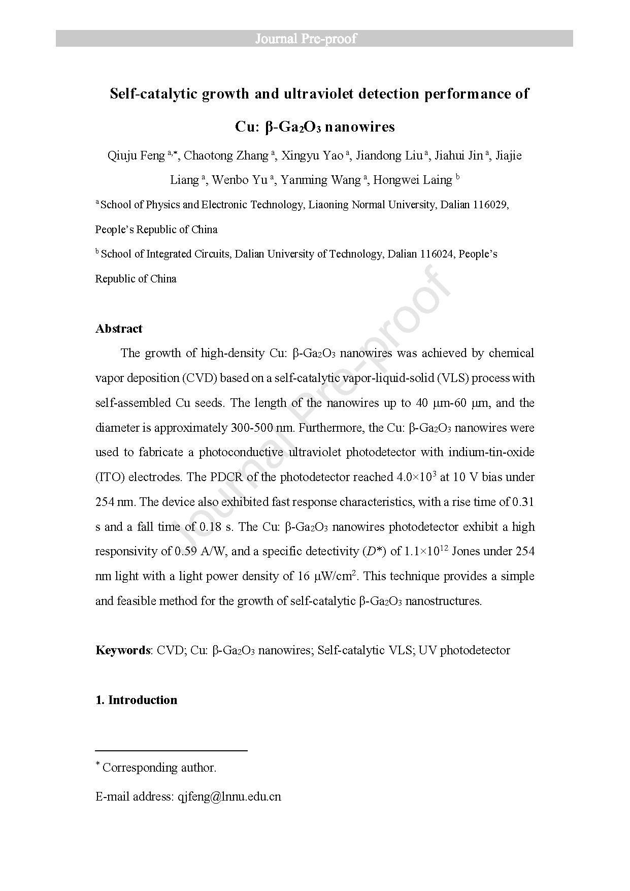
Fig. 1 Structrure schematic of photoconductive photodetector based on Cu: β-Ga2O3 nanowires.
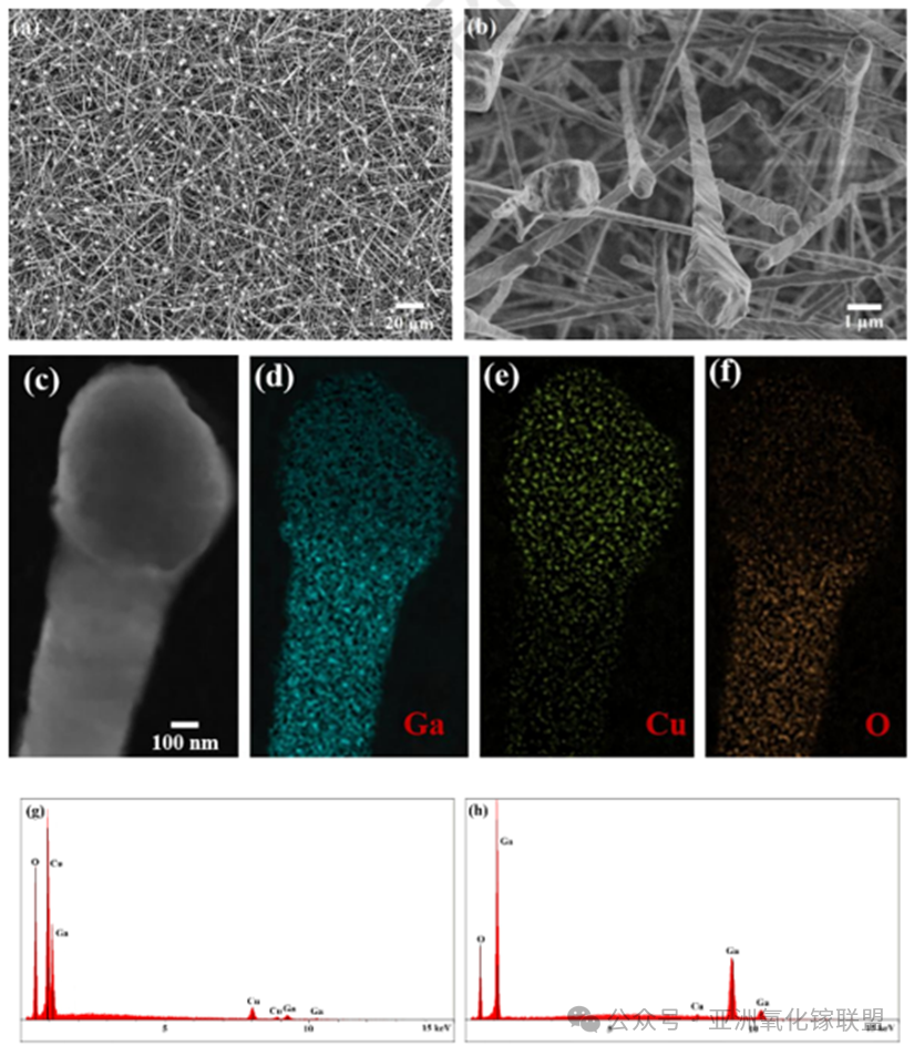
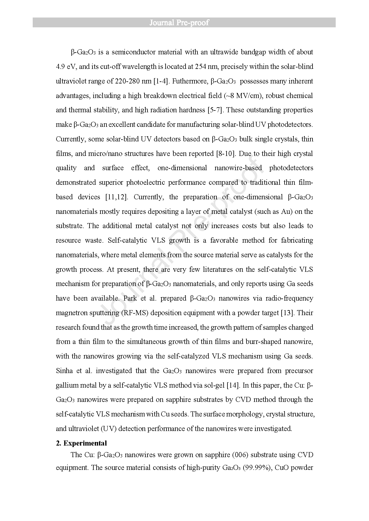
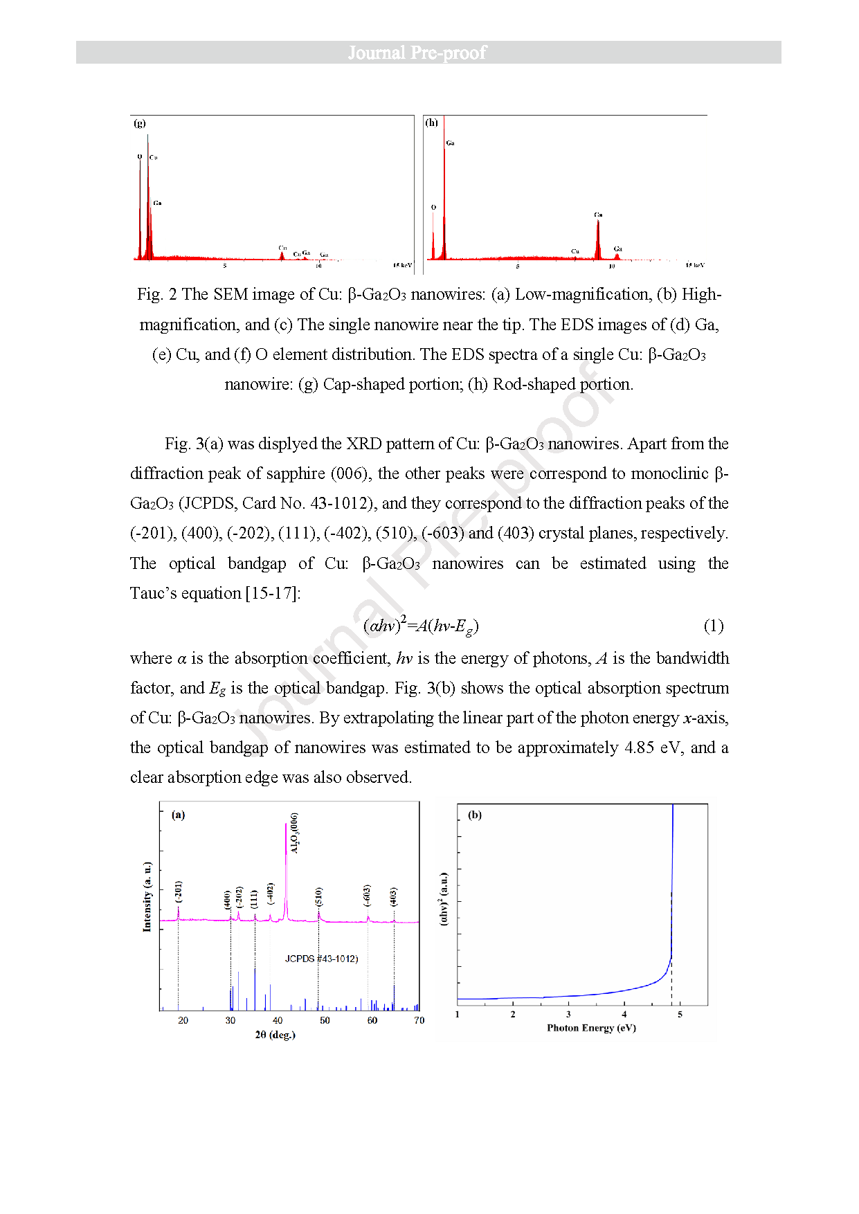
Fig. 2 The SEM image of Cu: β-Ga2O3 nanowires: (a) Low-magnification, (b) High-magnification, and (c) The single nanowire near the tip. The EDS images of (d) Ga, (e) Cu, and (f) O element distribution. The EDS spectra of a single Cu: β-Ga2O3 nanowire: (g) Cap-shaped portion; (h) Rod-shaped portion.
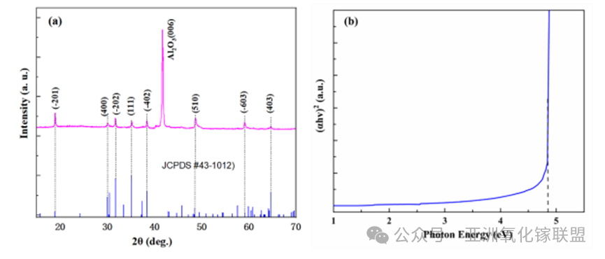
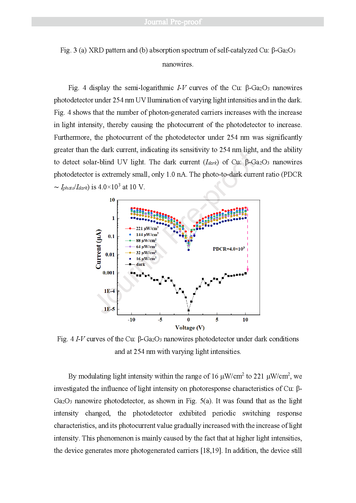
Fig. 3 (a) XRD pattern and (b) absorption spectrum of self-catalyzed Cu: β-Ga2O3 nanowires.
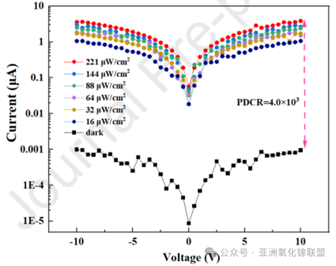
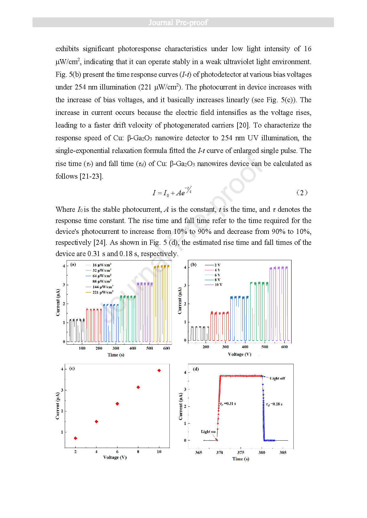
Fig. 4 I-V curves of the Cu: β-Ga2O3 nanowires photodetector under dark conditions and at 254 nm with varying light intensities.
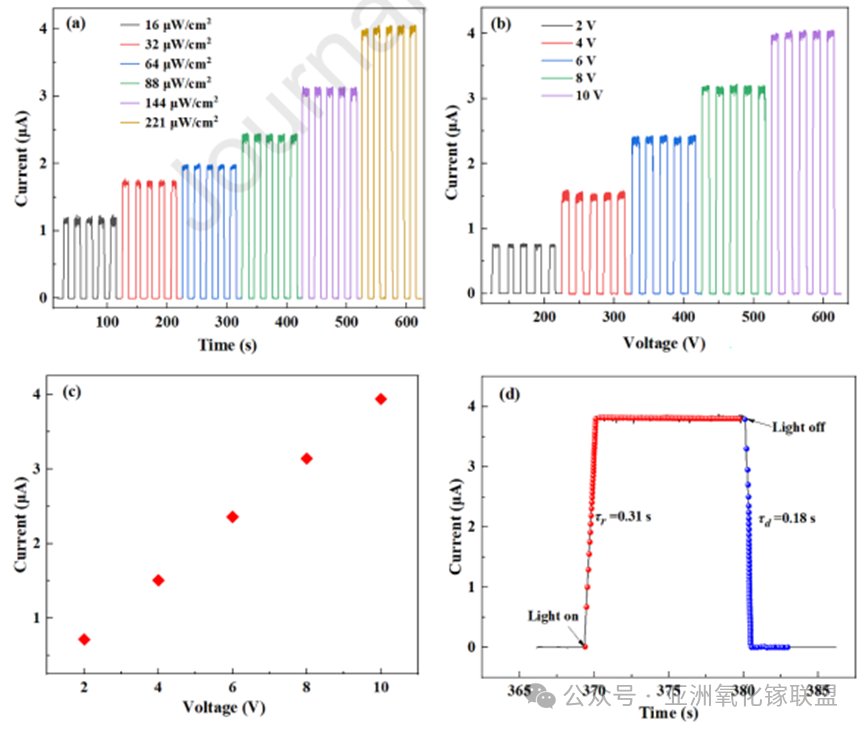
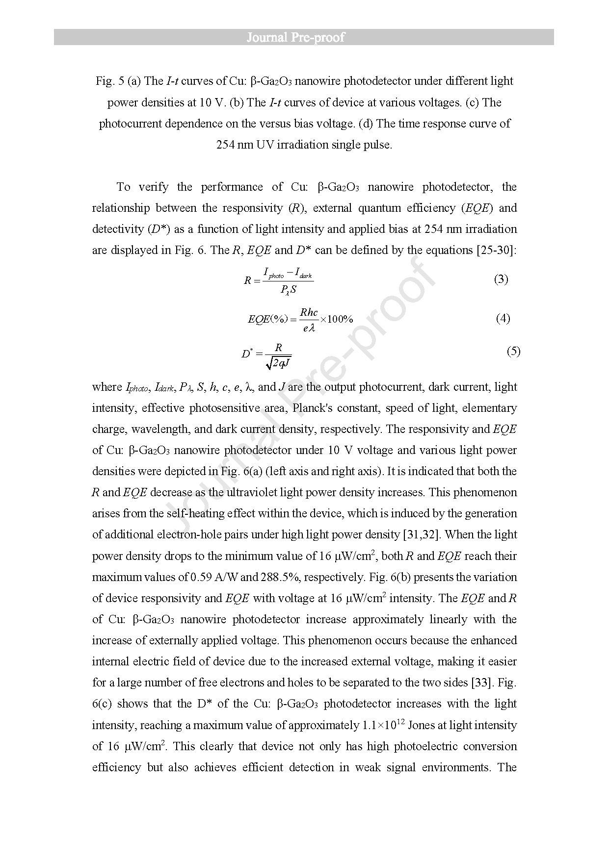
Fig. 5 (a) The I-t curves of Cu: β-Ga2O3 nanowire photodetector under different light power densities at 10 V. (b) The I-t curves of device at various voltages. (c) The photocurrent dependence on the versus bias voltage. (d) The time response curve of 254 nm UV irradiation single pulse.
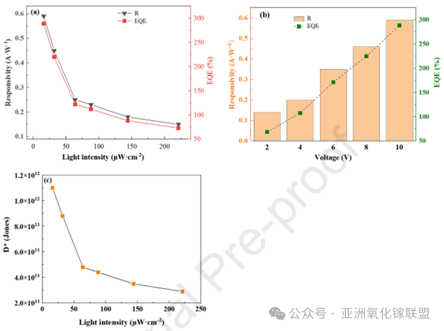
Fig. 6 The R and EQE of photodetector as a function of (a) light intensity and (b) bias voltage. (c) D* as a function of light intensity.
DOI:
doi.org/10.1016/j.physb.2026.418534