Paper Sharing
【Member Papers】Journal of Alloys and Compounds | Prof. Weifeng Yang’s Group at Xiamen University: Low-Leakage and High On/Off Current Ratio Vertical β-Ga₂O₃ Schottky Barrier Diodes Achieved by Interface Nitrogen Doping Technology
日期:2026-03-25阅读:175
A research team led by Prof. Weifeng Yang at Xiamen University has published a paper entitled “Low-Leakage and High On/Off Current Ratio Vertical β-Ga₂O₃ Schottky Barrier Diodes Induced by Interface Nitrogen Doping” in the international journal Journal of Alloys and Compounds.
Background
Gallium oxide (Ga₂O₃), as a fourth-generation ultra-wide bandgap semiconductor, possesses a large bandgap of approximately 4.8 eV and a high critical breakdown electric field of about 8 MV/cm, making it highly promising for high-voltage power electronics applications. Among various device types, Schottky barrier diodes (SBDs) have attracted significant attention due to their fast switching speed and low conduction loss, offering great potential for high-frequency and high-efficiency power conversion systems. However, the performance of Ga₂O₃ SBDs still falls far short of the theoretical limits of the material, mainly due to unresolved interface issues. On one hand, the Ga₂O₃ surface inherently contains a high density of defects, such as dangling bonds and oxygen vacancies, which introduce abundant interface states and lead to severe Fermi-level pinning, thereby limiting effective Schottky barrier modulation. On the other hand, fabrication processes can induce additional damage, resulting in trap-assisted leakage and local electric field crowding, which ultimately cause increased leakage current and premature breakdown. Although various interface treatment techniques, including plasma treatment, wet chemical cleaning, and thermal annealing, have been explored, these approaches often introduce new challenges such as secondary lattice damage, increased specific on-resistance, and complex processing steps. Therefore, developing a simple, low-damage, and effective interface engineering strategy that can simultaneously passivate defects and maintain device performance has become a critical scientific and technological challenge in Ga₂O₃ power electronics.
Abstract
To address these challenges, this work proposes and demonstrates an interface optimization strategy for Ga₂O₃ Schottky diodes based on atomic nitrogen doping. By introducing low-energy neutral nitrogen species to modify the device surface, the interface quality is effectively improved without inducing additional damage. Experimental results show that this method significantly enhances the overall electrical performance of the devices. Under a reverse bias of −200 V, the leakage current density is reduced from 10-4 A/cm² to 10-8 A/cm², while the on/off current ratio increases from 106 to 1010. Meanwhile, the specific on-resistance remains at 4.2 mΩ·cm² without degradation. The extracted Schottky barrier height increases after nitrogen doping, which explains the higher turn-on voltage and reduced leakage current.Time-of-flight secondary ion mass spectrometry (ToF-SIMS) results reveal enhanced signals of nitrogen-related species at the treated surface, while X-ray photoelectron spectroscopy (XPS) confirms the formation of Ga-O-N bonds and a reduction in oxygen vacancy concentration. In addition, the significant reduction in interface state density alleviates Fermi-level pinning, enabling effective modulation of the Schottky barrier height. The simultaneous improvement in leakage current and breakdown voltage is attributed to the synergistic effects of interface state reduction, oxygen vacancy passivation, and Schottky barrier modulation. This work highlights the strong potential of atomic nitrogen doping for high-performance Ga₂O₃ power devices.
Highlights
Atomic nitrogen doping enables low-damage interface engineering of Ga₂O₃.
Low-energy nitrogen species prevent lattice damage while maintaining low on-resistance.
Multi-technique characterization verifies nitrogen incorporation and defect suppression mechanisms.
Conclusion
This work systematically investigates and verifies the effectiveness of atomic nitrogen doping for Schottky interface engineering in Ga₂O₃. The results demonstrate that this approach can significantly enhance device performance without introducing additional damage. Electrical measurements show that the treated devices exhibit a substantial reduction in reverse leakage current and a notable improvement in breakdown voltage while maintaining a low specific on-resistance, indicating excellent rectification behavior and electrical stability. Further analysis using ToF-SIMS and XPS reveals that nitrogen atoms are primarily distributed within a nanoscale region near the surface and form stable Ga-O-N bonds, which effectively passivate intrinsic defects such as oxygen vacancies and significantly reduce the interface state density. The reduction of interface defects not only alleviates Fermi-level pinning but also increases the Schottky barrier height, enabling carrier transport closer to the ideal thermionic emission mechanism while suppressing trap-assisted conduction. These improvements lead to modulation of the space-charge region and reduction of local electric field crowding, thereby enhancing the breakdown capability of the devices. Overall, atomic nitrogen doping achieves a synergistic optimization of leakage current, breakdown voltage, and conduction performance through defect passivation, interface state suppression, and barrier engineering. This study provides a simple, effective, and process-compatible solution for interface engineering in Ga₂O₃ power devices and offers valuable insights for pushing device performance closer to the material limits.
Project Support
This work was supported by the National Natural Science Foundation of China (Grant No. 62171396) and the Shenzhen Science and Technology Program (Grant No. JCYJ20240813145617023).
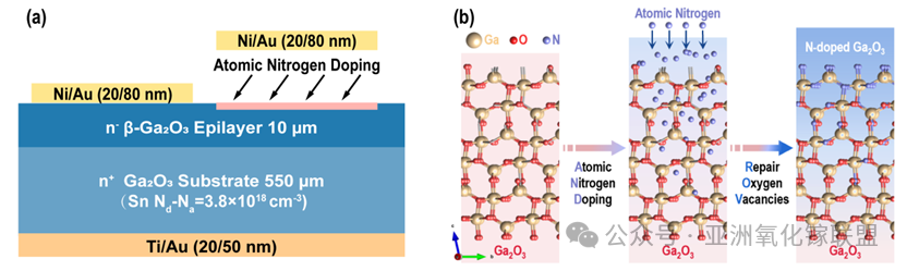
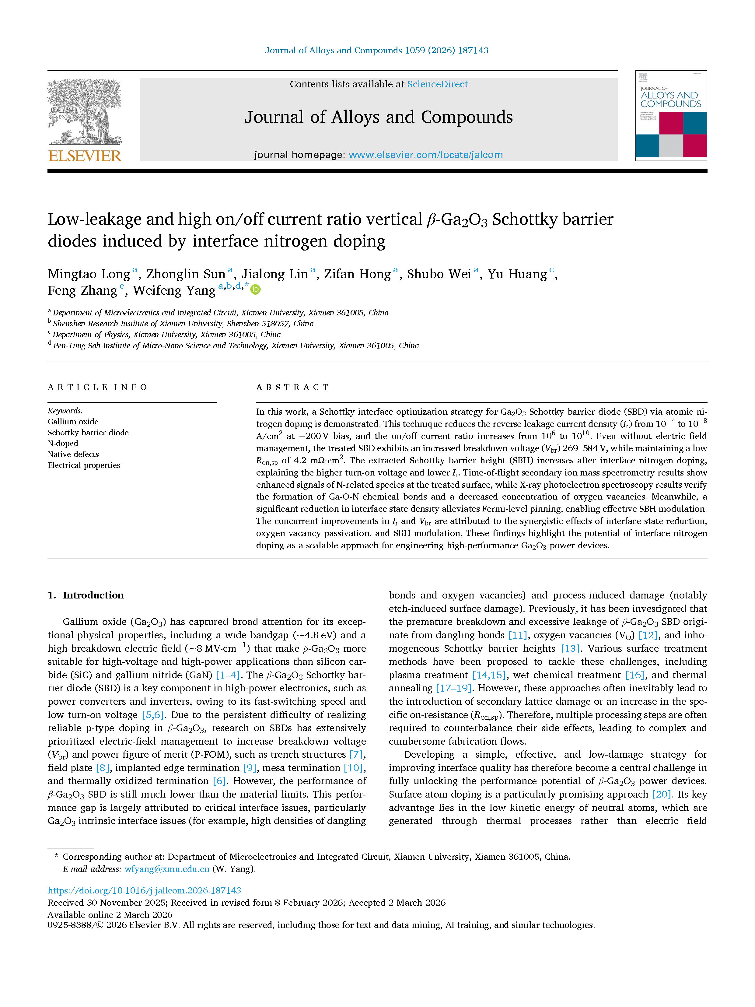
Figure 1. a) Schematic cross-section of the REF-SBD and AND-SBD. b) Schematic illustration of the atomic nitrogen-doping on the β-Ga2O3.
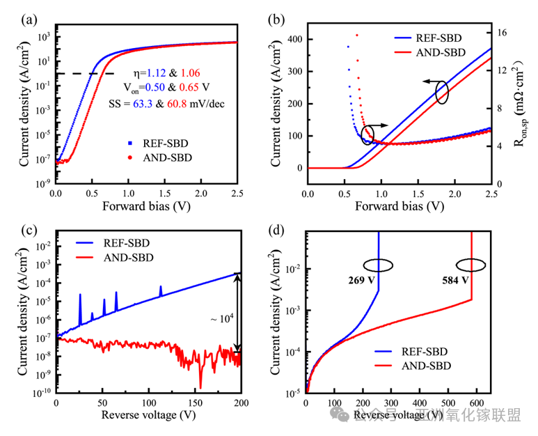
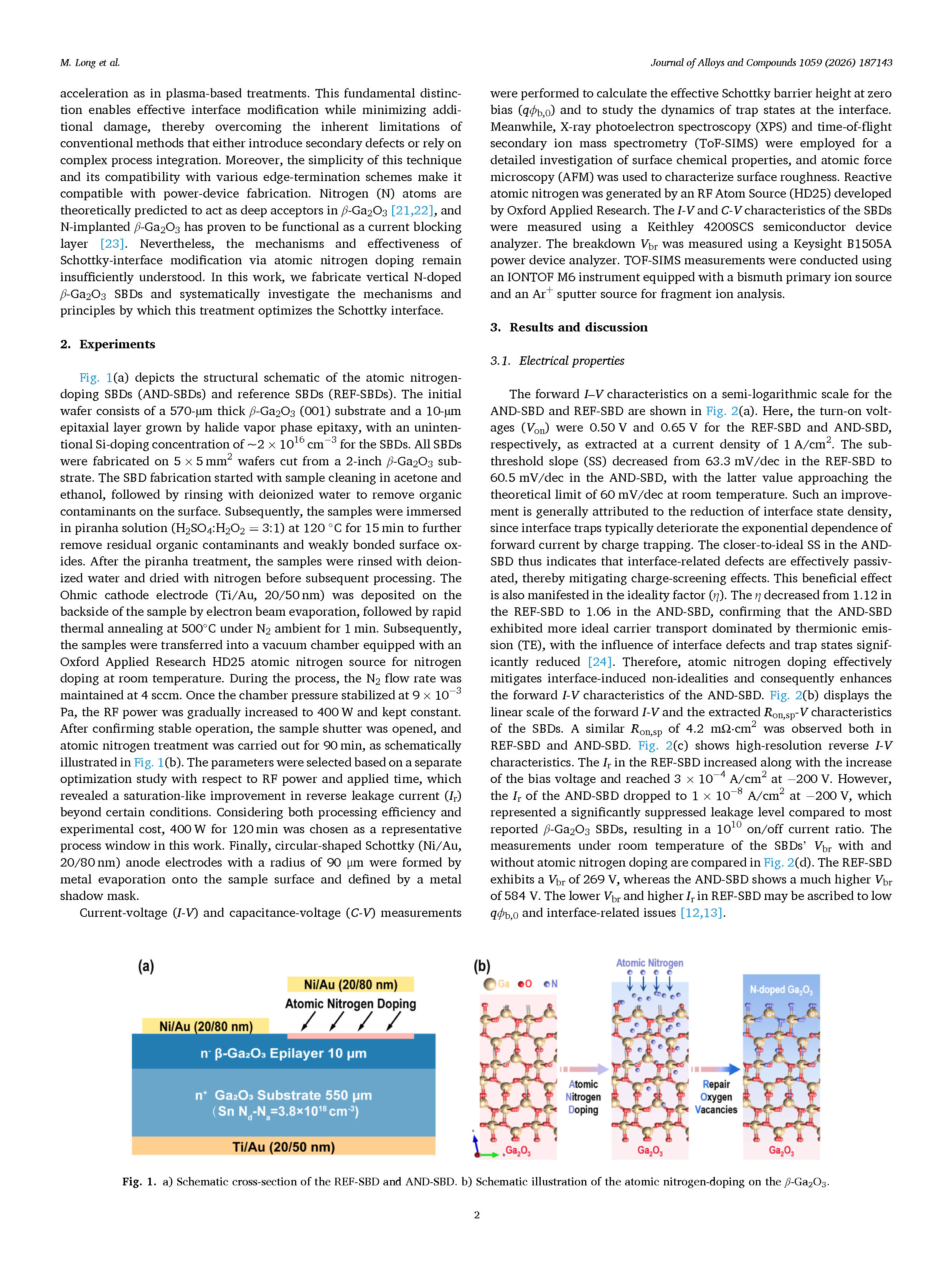
Figure 2. a) Semi-log plot of forward I-V characteristics of the REF-SBD and AND-SBD. b) Linear-scale plot of forward I-V characteristics and extracted Ron,sp-V characteristics of the SBDs. c) The high-resolution reverse I-V characteristics. d) Breakdown voltage of the REF-SBD and AND-SBD.
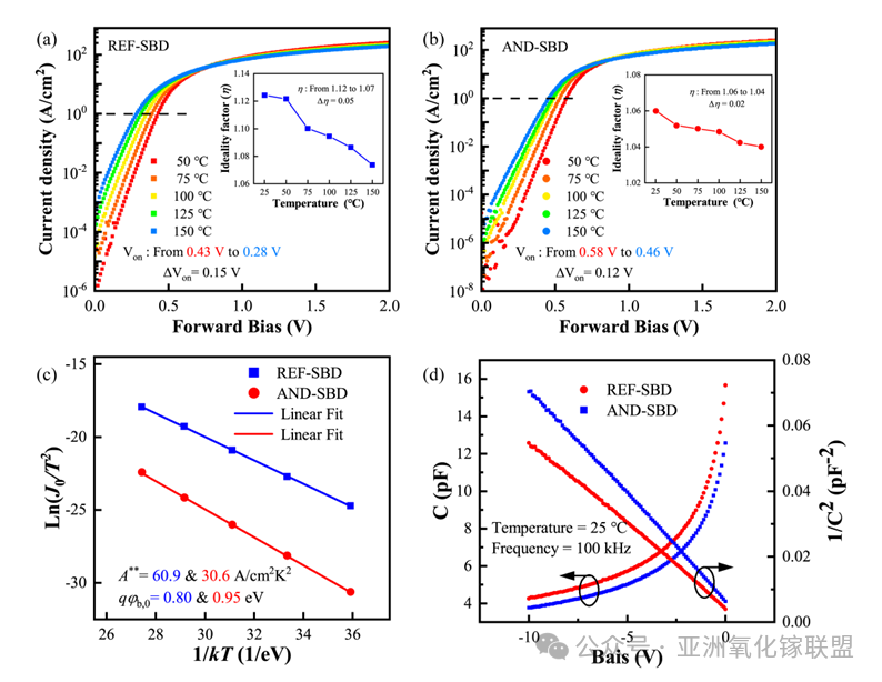
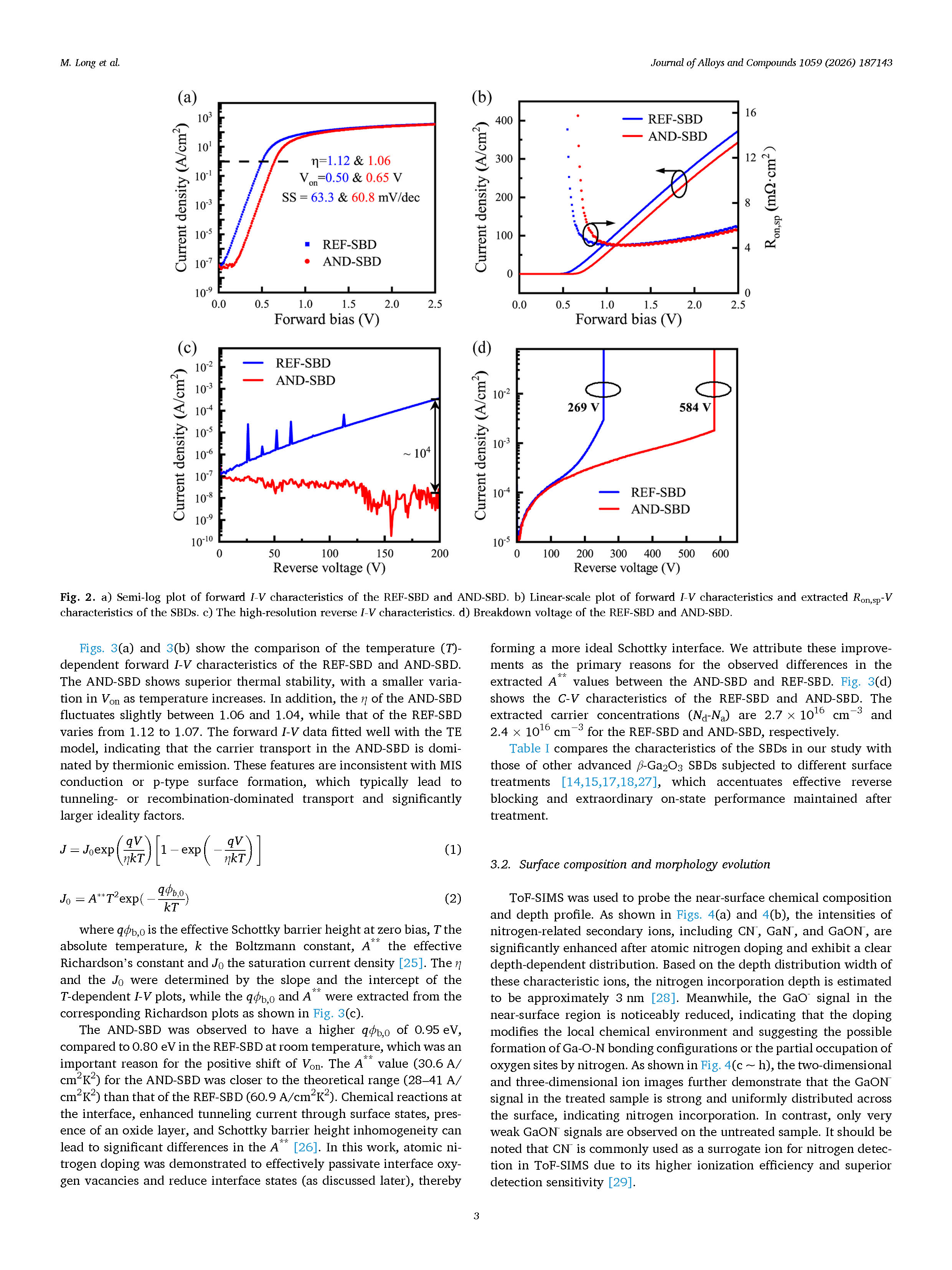
Figure 3. T-dependent forward I-V characteristics of the a) REF-SBD and b) AND-SBD tested from 50℃ to 150℃. The temperature dependence of the ideality factor is plotted in the inset. c) The corresponding Richardson’s plot of the SBDs. d) The measured C-V and 1/C2-V curves of the SBD.
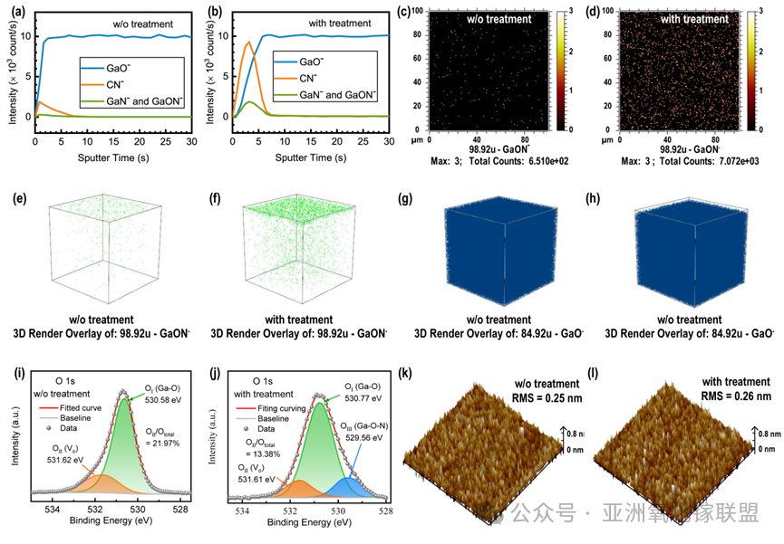
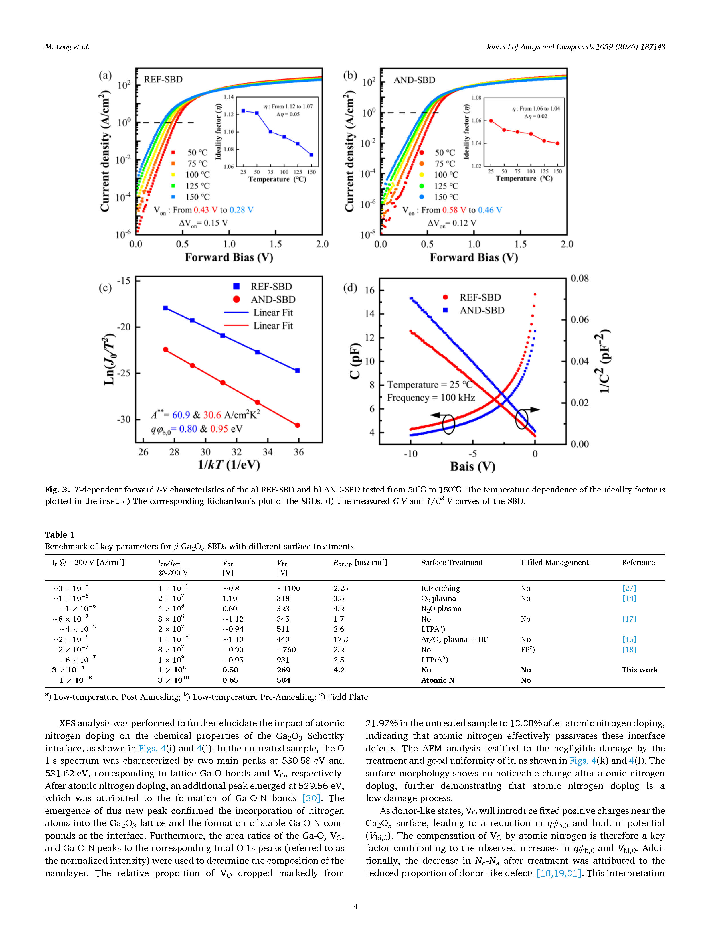
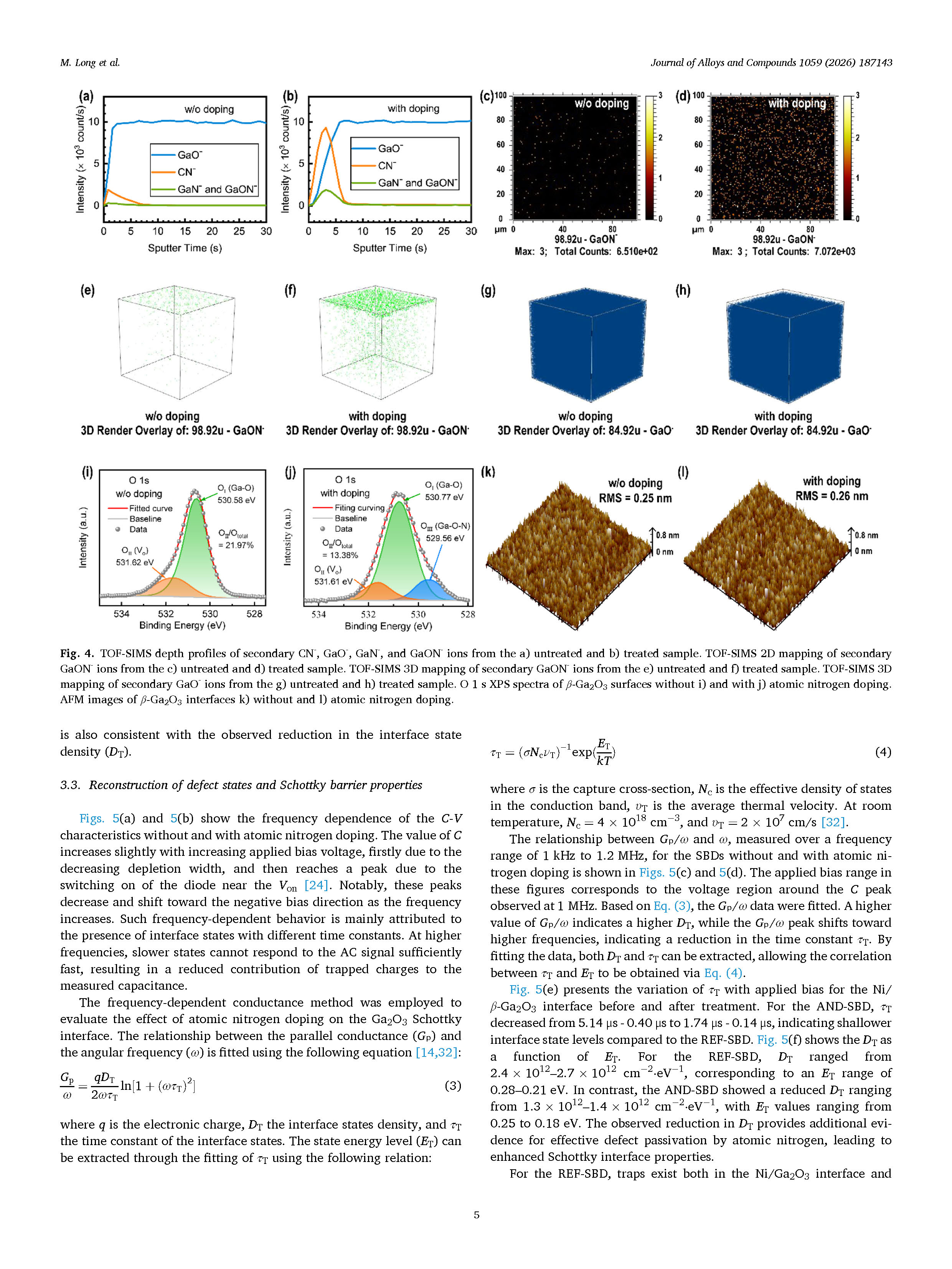
Figure 4. TOF-SIMS depth profiles of secondary CN-, GaO-, GaN-, and GaON- ions from the a) untreated and b) treated sample. TOF-SIMS 2D mapping of secondary GaON- ions from the c) untreated and d) treated sample. TOF-SIMS 3D mapping of secondary GaON- ions from the e) untreated and f) treated sample. TOF-SIMS 3D mapping of secondary GaO- ions from the g) untreated and h) treated sample. O 1s XPS spectra of β-Ga2O3 surfaces without i) and with j) atomic nitrogen doping. AFM images of β-Ga2O3 interfaces k) without and l) atomic nitrogen doping.
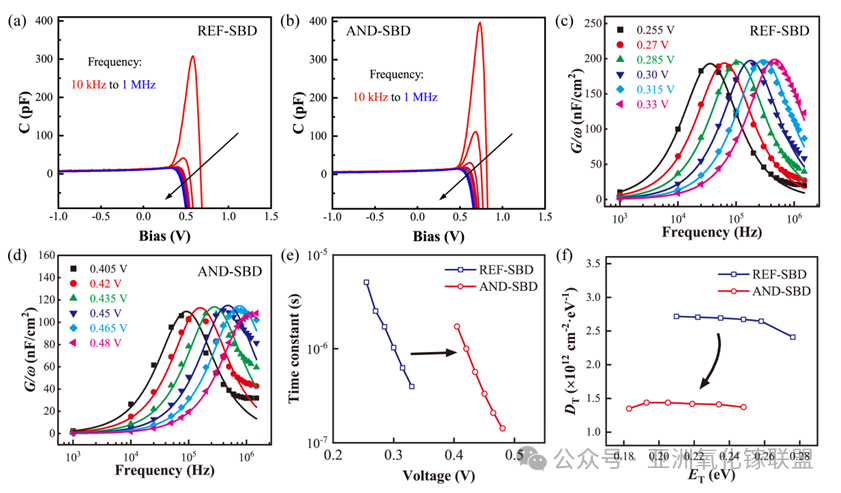
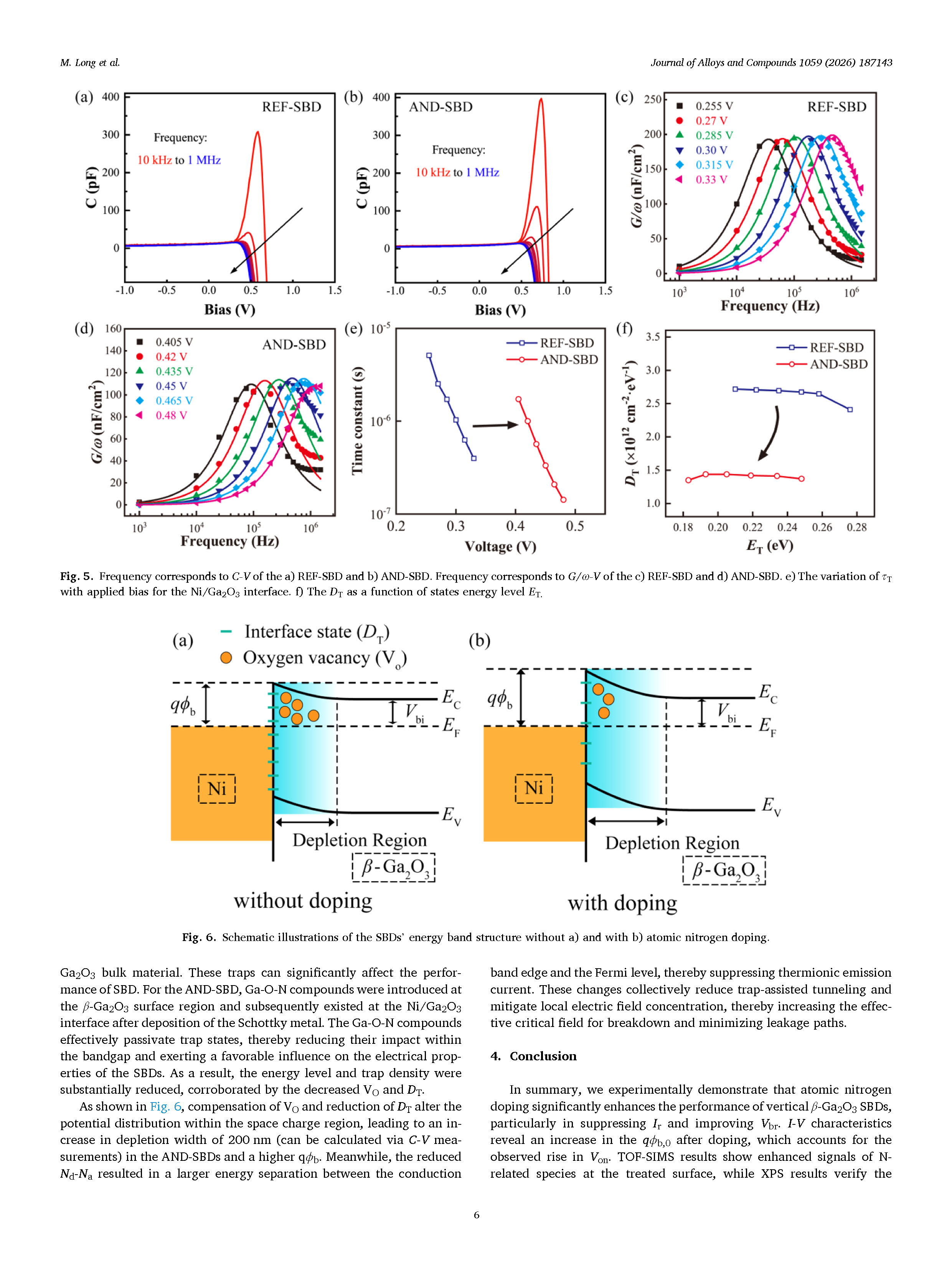
Figure 5. Frequency corresponds to C-V of the a) REF-SBD and b) AND-SBD. Frequency corresponds to G/ω-V of the c) REF-SBD and d) AND-SBD. e) The variation of τT with applied bias for the Ni/Ga2O3 interface. f) The DT as a function of states energy level ET.
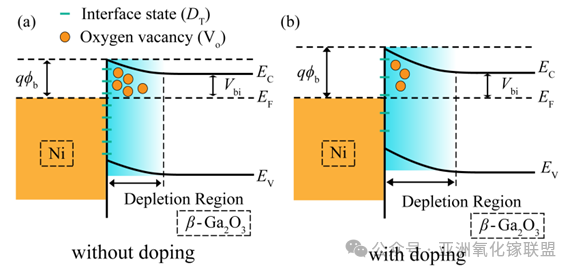
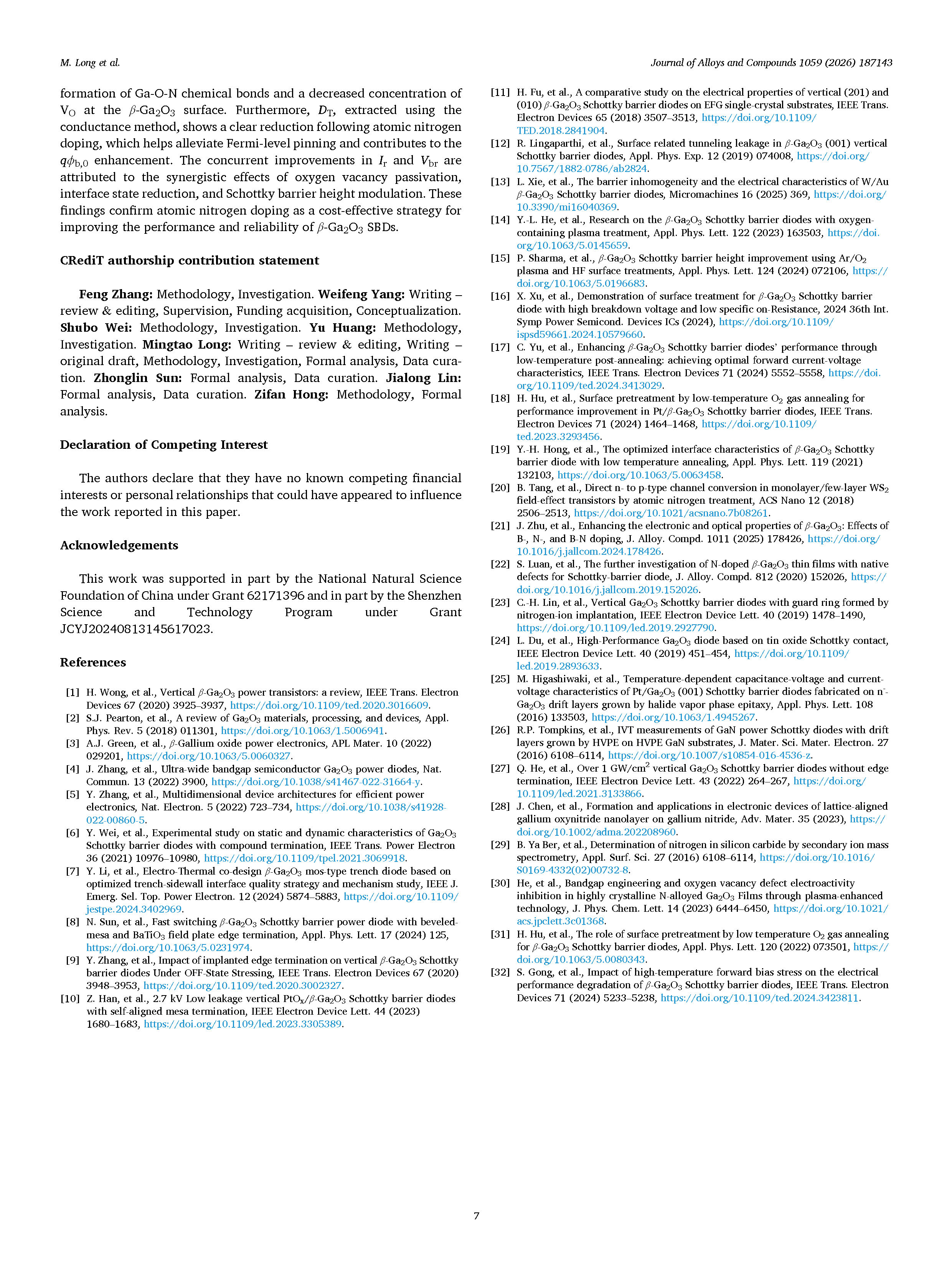
Figure 6. Schematic illustrations of the SBDs’ energy band structure without a) and with b) atomic nitrogen doping.
DOI:
doi.org/10.1016/j.jallcom.2026.187143