


Member News
【Member News】Authoritative Validation!GAREN SEMI' s 8-lnchHomoepitaxial Gallium Oxide Wafers Deliver Outstanding Performance with Globally Leading Key Metrics
日期:2026-03-24阅读:280
In March 2026, the 8-inch homoepitaxial Gallium Oxide wafers developed by Hangzhou Garen Semiconductor Co., Ltd. (hereinafter referred to as “Garen Semiconductor”) successfully passed authoritative certification by the Shenzhen Pinghu Laboratory.
Test results indicate that the key performance metrics of Garen’s 8-inch Gallium Oxide homoepitaxial wafers are outstanding, with some parameters reaching internationally leading levels, laying a solid foundation for the industrialization of Gallium Oxide devices.
Authoritative Testing: Excellent Performance in Key Metrics
In this evaluation, the Pinghu Laboratory conducted combined AFM (Atomic Force Microscopy) and XRD (X-ray Diffraction) measurements on five key points of an 8-inch homoepitaxial Gallium Oxide wafer developed by Garen Semiconductor.
The XRD rocking curve full width at half maximum (FWHM) values at the center and the upper and lower points ranged from 30 to 46 arcsec, representing an excellent level. Notably, the left and right points achieved FWHM values of only 21.18 arcsec and 22.18 arcsec, respectively, both reaching a globally leading level.
The epitaxial wafer exhibits highly ordered lattice arrangement and extremely low defect density, fully meeting the application requirements for ultra-high-voltage and high-power devices.
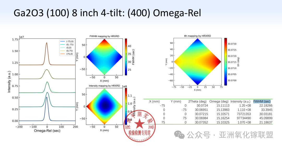
Figure 1. XRD characterization results of the 8-inch Gallium Oxide homoepitaxial wafer from Garen Semiconductor
In the AFM surface roughness measurements, the left-side point of the epitaxial wafer shows an Rq as low as 0.144 nm and an Ra of only 0.115 nm. The upper point exhibits an Rq of 0.168 nm and an Ra of 0.134 nm. These two key regions demonstrate excellent surface flatness, meeting the standards for high-end Gallium Oxide epitaxial wafers and providing a high-quality surface foundation for subsequent device fabrication.
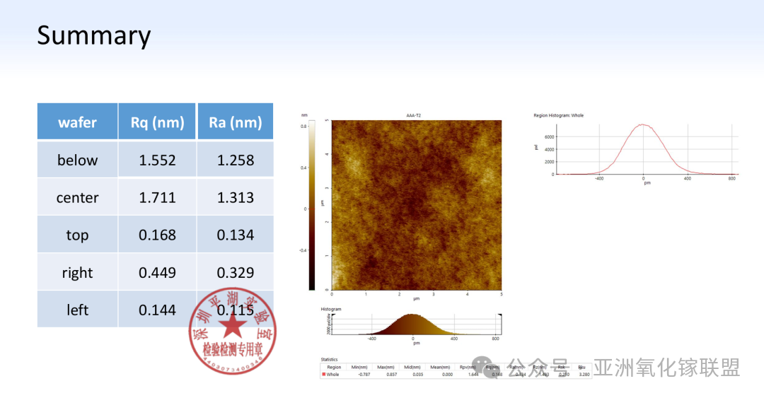
Figure 1. XRD Characterization Results of Garen Semiconductor’s 8-inch Gallium Oxide Homoepitaxial Wafer (Part 2)
Key Interpretation: Homoepitaxy as the Optimal Path
Gallium Oxide, as a core material of the fourth-generation ultra-wide bandgap semiconductors, demonstrates significant advantages in high-end power device applications. Large-size epitaxial wafers are a key enabler for its industrialization.
Heteroepitaxial growth methods, due to the mismatch between substrate and epitaxial materials, inherently suffer from lattice mismatch and interface defects, preventing full realization of Gallium Oxide’s intrinsic advantages.
Homoepitaxy, as the optimal route for Gallium Oxide epitaxy, holds critical significance in three aspects:
Perfect lattice matching, unlocking intrinsic material advantages:
Homoepitaxy completely eliminates lattice mismatch and stress concentration issues found in heteroepitaxy, significantly reducing defect density and enabling the full potential of Gallium Oxide in ultra-high-voltage and low-loss applications.
Ensuring high device performance and overcoming industrialization bottlenecks:
The surface flatness and crystalline quality of homoepitaxial layers are easier to control, addressing key challenges of heteroepitaxial devices such as insufficient breakdown voltage and poor reliability, thereby supporting large-scale mass production.
Simplified process and cost reduction, enhancing industrial competitiveness:
Homoepitaxial growth does not require additional buffer layers, simplifying the process and reducing defect mitigation costs. Compared with heteroepitaxy, it offers superior feasibility for industrial-scale deployment.
Significance of the Breakthrough and Future Outlook
This authoritative validation fully demonstrates Garen Semiconductor’s precise control over large-size homoepitaxial growth processes, overcoming the long-standing industry challenge of balancing wafer size and material quality. It further confirms that homoepitaxy is currently the only viable path for the industrialization of Gallium Oxide.
Garen Semiconductor’s breakthrough in Gallium Oxide homoepitaxial growth technology effectively fills a gap in the ultra-wide bandgap semiconductor field and enhances the company’s global competitiveness in the fourth-generation semiconductor sector.
Looking ahead, Garen Semiconductor’s R&D team will continue to optimize processes and improve intra-wafer uniformity, driving further advancements in Gallium Oxide technology. These efforts actively align with the strategic priorities outlined in China’s 15th Five-Year Plan regarding Gallium Oxide industry development, contributing to the sustained growth of the semiconductor industry and the advancement of technological self-reliance.
About GAREN SEMI
Hangzhou Garen Semiconductor Co., Ltd. is a world-leading provider of Gallium Oxide materials and equipment solutions, focusing on R&D and industrialization in the ultra-wide bandgap semiconductor field. The company’s core products include 2–8-inch Gallium Oxide single crystals and substrates (with 8-inch being the world’s first), Gallium Oxide Vertical Bridgman (VB) crystal growth equipment, Gallium Oxide epitaxial wafers, etc. It is committed to building a full-chain product system of “equipment–crystal–substrate–epitaxy” to provide systematic solutions for global customers. The company’s achievements in Gallium Oxide have been specially reported by well-known media including People’s Daily, Xinhua News Agency, Science and Technology Daily, Sina Finance, China Blue News, and The Paper.
Enterprise Honors Summary
Recognized as a National-level Science and Technology Small and Medium-sized Enterprise and Zhejiang Innovative Small and Medium-sized Enterprise in 2023;Awarded Zhejiang Specialized, Sophisticated, Unique and New Small and Medium-sized Enterprise in 2024;Approved as a High-tech Enterprise in 2025;Won the SEMI Outstanding Contribution Award for Sustainable Development at SEMICON CHINA 2025, the Together Progress Award at the Jufeng Summit Forum (JFSC) and Compound Semiconductor Industry Expo, the Innovation Vitality Award of Zhejiang Semiconductor Industry, the Second Prize in the Enterprise Group of the 10th “Maker China” Zhejiang Provincial Finals, the Top 500 Enterprise Group of the 10th “Maker China” SME Innovation and Entrepreneurship Competition, and the 2024–2025 Semiconductor Material Industry Contribution Award;The major breakthrough in the preparation of 8-inch Gallium Oxide single crystals and substrates was selected as one of the “Top 10 Advances in China’s Third-Generation Semiconductor Technology 2025” and “Major Scientific and Technological Achievements 2025” by the Department of Science and Technology of Zhejiang Province;Led the formulation of 2 group standard drafts, participated in drafting 1 national standard, and participated in promoting 1 group standard draft in the Gallium Oxide field;Supported by the “5213” Excellence Program of Xiaoshan District, Hangzhou, Zhejiang Province, and approved to establish Zhejiang Enterprise Research Institute;Obtained the quality management system certification;Granted 14 authorized invention patents at home and abroad (including patents in the US, Japan and other countries), with more than 50 patents pending.
For more information about Garen Semiconductor and its products, please visit our official website: http://garen.cc/
Or contact us via the following ways:
Mr. Jiang: 15918719807
E-mail: jiangjiwei@garen.cc
Mr. Xia: 19011278792
E-mail: xianing@garen.cc
