Expert Interview
【Expert Interview】From Technology to Industry: Prof. Tang Weihua Elaborates on GAO SEMI’s Systematic Layout and Future Plans for Gallium Oxide
日期:2025-12-05阅读:905
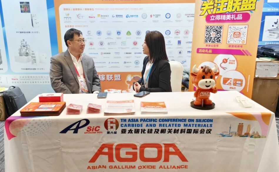
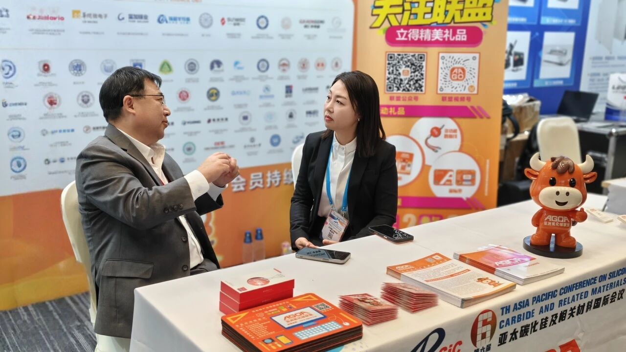
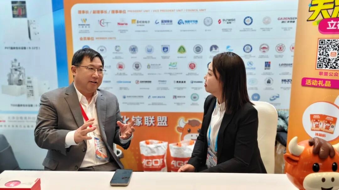
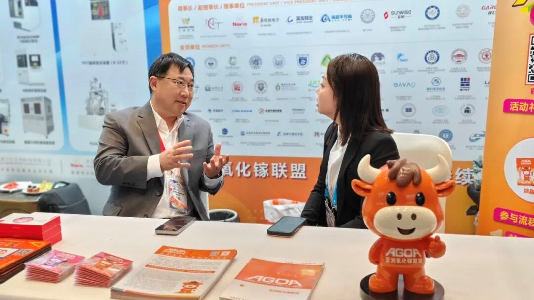
At the 6th Asia-Pacific Conference on Silicon Carbide and Related Materials (APCSCRM 2025), Gallium Oxide emerged as one of the core focal points within the industry. As an invited participant, Asian Gallium Oxide Alliance (AGOA) conducted a dedicated interview during the conference with Prof. Wei-Hua Tang, Chairman of GAO Semiconductor, focusing on the company’s systematic deployment and future strategies in the Gallium Oxide field.
The interview centered on GAO SEMI’s comprehensive layout, technological innovation, and industrialization progress in Gallium Oxide, clarifying its integrated development path of “substrate – epitaxy – device”, highlighting the potential of both optoelectronic and power device applications. GAO SEMI has set its 2026 objectives toward technological upgrading, production stability, and achieving self-sustaining growth. Prof. Tang also suggested that the Alliance should continue to play a pivotal role in areas such as technology iteration, industry coordination, ecosystem cultivation, resource matchmaking, and talent development, jointly accelerating the industrialization of Gallium Oxide.
1. Founding Motivation, Company Layout, and Current Progress
Founding Motivation
The original intention behind Professor Tang’s establishment of an industrialization-oriented company stems from long-standing challenges encountered in earlier research. At that time, Gallium Oxide substrates and epitaxial wafers required for experimental projects were extremely expensive, had long delivery cycles, and more critically, the entire supply chain was under foreign control. This persistent “bottleneck” drove Professor Tang to begin with epitaxy and undertake systematic fundamental research on the intrinsic properties of Gallium Oxide materials.
GAO SEMI set two explicit goals from the outset:
(1) To break foreign technological monopolies and achieve independent control of key semiconductor materials, and
(2) To build, deepen, and advance the entire Gallium Oxide material system, contributing to China’s foundational semiconductor technology capabilities.
Company Layout
In its overall strategic layout, GAO Semiconductor has consistently focused on Gallium Oxide substrates, a foundational and mission-critical material in the semiconductor industry. At present, GAO SEMI’s Gallium Oxide substrate product line has achieved comprehensive coverage of 2-inch, 4-inch, and 6-inch sizes, with R&D efforts continuously directed toward quality enhancement.
Specifically, GAO SEMI has achieved twin-free growth for 4-inch crystals; meanwhile, the 6-inch (100)-oriented crystals and 2-inch (001)-oriented crystals have also largely resolved twin-crystal issues. Among these products, the 4-inch substrates are ready for mass production and can be downward-compatible with 2-inch device fabrication. The 6-inch substrates are currently undergoing process optimization to further improve yield and stability.
Since its founding, the company has invested in the development of epitaxy and power devices, though earlier progress was constrained by limitations in substrate supply. Now, with fully self-supported substrate production, GAO SEMI has restarted and expanded its epitaxy business:
Heteroepitaxy is primarily oriented toward optoelectronic applications, with close collaboration established with domestic universities and research institutes.
Homoepitaxy is centered on 2-inch substrates, and GAO SEMI is working with key downstream customers on joint development.
GAO SEMI is evolving from a single substrate supplier into an integrated platform providing full-chain technological services and collaborative innovation across “substrate – epitaxy – device applications.” The company is committed to serving as a crucial bridge linking industry, education, research, and application, accelerating the translation and deployment of Gallium Oxide technologies.
Current Progress
In terms of industrialization progress, leveraging its team’s years of technical expertise in optoelectronic devices, Suzhou GAO SEMI has successfully advanced Gallium Oxide–based photodiodes and focal plane array (FPA) detectors toward engineering verification and productization. These application-oriented products have passed authoritative industry testing and have been validated by downstream users, demonstrating strong market potential.
GAO SEMI maintains firm confidence in the long-term development prospects of Gallium Oxide in power electronics and deep-ultraviolet optoelectronics, while also recognizing that industrialization is a highly systematic endeavor. It requires holistic planning, tightly linked processes, and steady advancement—from materials, epitaxy, and device fabrication to end-application integration, with each step being indispensable.
Among these factors, deep engagement and co-innovation with key downstream customers serve as the essential driving force propelling Gallium Oxide industrialization forward. GAO SEMI will continue to follow a dual-path strategy that emphasizes both technological independence and open collaboration, working together with industry partners to accelerate the maturation and expansion of the Gallium Oxide ecosystem.
2. Opportunities, Challenges, and Commercialization Timeline of Gallium Oxide Industrialization
In the industrialization of Gallium Oxide, the primary challenges faced by GAO SEMI arise from the systemic and highly coordinated nature of semiconductor technological development. In the semiconductor industry, equipment, materials, and fabrication processes are deeply interconnected. For Gallium Oxide, breakthroughs on the materials side fundamentally depend on the maturity of the process, while process optimization must in turn drive iterative upgrades of dedicated equipment.
This means that Gallium Oxide industrialization cannot advance by isolating individual segments; it requires synchronized development and closed-loop feedback across “process–equipment–application”, followed by continuous optimization.
For example, once Gallium Oxide enters a stage of large-scale commercialization, stable and reliable mass-production growth equipment will become indispensable. This requires GAO SEMI, at the current stage, to continuously feed process know-how back into equipment development through its enterprise platform, enabling targeted improvements and multiple rounds of iteration to achieve long-term controllability and stable yield in mass production.
At present, the Gallium Oxide industry remains in the R&D and early-adoption phases. Companies must actively fill numerous technological gaps, build independent process systems, and ensure high-quality material standards. Meanwhile, maintaining strategic discipline is essential—avoiding the temptation of short-term market trends and instead focusing on deep accumulation and long-term optimization of foundational technologies.
In terms of technical pathways, the mainstream direction for large-diameter Gallium Oxide substrates in China focuses on the (100) orientation. The (100) orientation shows higher breakdown-voltage potential for power electronics, and institutions such as Germany’s IKZ continue to invest heavily in this direction. GAO SEMI has established clear quality-control standards for its substrate products:
Twinning-free materials;
No micropipes;
Excellent surface-processing quality.
GAO SEMI emphasizes that substrate quality is not limited to bulk material metrics. Its compatibility with epitaxial processes—especially surface quality—has a decisive impact on subsequent epitaxy and device performance, and is fundamental to real industrial application.
Regarding the timeline for commercialization, GAO SEMI believes the process is inherently gradual and tightly coupled with process maturity, equipment capability, and downstream application pull. True large-scale adoption of Gallium Oxide requires material cost, wafer size, and long-term reliability to meet the thresholds of mass-market deployment—an outcome dependent on close collaboration across the entire industry chain.
GAO SEMI anticipates that within the next 3–5 years, Gallium Oxide will achieve breakthroughs from technology validation to initial commercial adoption in several specialized sectors. However, widespread industrial penetration will require longer-term technological accumulation and ecosystem development.
GAO SEMI will continue focusing on independent innovation of core materials technologies, working closely with its partners to pragmatically advance the healthy and steady development of the Gallium Oxide industry.

3. Comparative Potential and Market Positioning of Gallium Oxide for Photonic and Power Devices
In the industrialization of Gallium Oxide, both the photonic-device direction and the power-device direction exhibit clear development potential and distinct market positioning. Together they form the two principal pillars of the company’s technology strategy.
Photonic-device direction: centered on solar-blind detectors
This direction leverages Gallium Oxide’s intrinsic absorption in the deep-ultraviolet band to develop high-sensitivity, high-reliability UV photodetectors. Its core strengths lie in device stability and system safety, making it particularly well suited for industrial scenarios that require non-contact safety monitoring—such as new energy systems, power grid monitoring, and energy storage cabinets. Within the photonic submarket, solar-blind detectors possess irreplaceable performance advantages: a clear market positioning, obvious application prospects, and broad future demand. GAO SEMI has already built an integrated R&D and manufacturing capability encompassing substrate → epitaxy → photonic devices, and its related products have progressed from technology development to productization.
Power-device direction: focused on high breakdown voltage and low loss
This direction exploits Gallium Oxide’s extremely high critical breakdown field to develop the next generation of high-voltage, high-efficiency power electronic devices. Notably, (100)-oriented Gallium Oxide substrates have demonstrated higher breakdown voltage potential in experiments, matching the core voltage-withstand requirements of power devices. In terms of industrialization pathways, Japan has already advanced along a “substrate → epitaxy → Schottky barrier diode (SBD)” route; domestically, research teams such as those at Xidian University and Sun Yat-sen University are actively exploring Gallium Oxide-based RF device extensions and related fields.
On development philosophy and positioning
GAO SEMI believes that technical accumulation requires patience and resilience through cyclical challenges. As exemplified by the company’s founder, Professor Tang, who committed to Gallium Oxide research during his early years at Beijing University of Posts and Telecommunications—focusing on the material for many years since 2011—this long-term dedication underpins the company’s capacity for sustained innovation and steady progress. In market competition, GAO SEMI recognizes that while the overall photonics market size may be modest, the advantages and market prospects for solar-blind detectors are significant and well aligned with the company’s integrated capabilities. Conversely, the power-device sector has vast potential but still requires substantial process maturity and ecosystem cultivation. Therefore, during the R&D stage the company advocates maintaining technical openness and exploring multiple avenues for breakthroughs, but ultimately insists on returning to product-oriented industrialization. True competitive advantage stems from robust technology and dependable products that enable sustainable operation—not from capital alone or simply pursuing larger crystal sizes as a headline metric.
GAO SEMI will continue to concentrate on core material technologies, methodically building an independent intellectual property portfolio across both directions, proceeding with meticulous, pragmatic steps to promote Gallium Oxide’s first-mover applications and long-term iterative improvement in selected fields.
4. Goals of GAO SEMI for 2026
In 2026, GAO SEMI will continue to advance its work systematically across materials & technology and industrialization & market deployment, further consolidating its core strengths and industry position in the gallium oxide sector.
Materials & Technology Development
[1] Deepening collaboration on 4-inch substrates with downstream key device manufacturers.
By establishing joint R&D mechanisms, co-validation platforms, and long-term technical cooperation models, the company aims to accelerate material–device compatibility, shorten development cycles, and drive iterative upgrades in terminal applications.
[2] Addressing the challenges of process stability and uniformity for 6-inch substrates.
GAO SEMI will concentrate resources on enabling a solid transition of 6-inch Gallium Oxide substrates from technology development to engineering and productization.
The goal is to achieve stable supply of high-quality wafers and deliver systematic breakthroughs across key performance indicators, laying the foundation for large-scale industrial adoption.
Industrialization & Market Deployment
2026 will be a critical year for GAO SEMI to strengthen its market capabilities and establish a sustainable, self-supporting operational system.
The company will elevate sales system development and commercial application deployment to strategic priorities, including:
● Expanding downstream application channels
● Accelerating standardized adoption and large-scale deployment among key customers and benchmark scenarios
● Strengthening market-driven product planning
● Optimizing the product portfolio
● Enhancing customer experience and integrated service capabilities
Through these efforts, GAO SEMI aims to build a robust commercial and operational flywheel, enabling sustainable revenue generation and contributing long-term momentum to the development of the Gallium Oxide industry.
5. Recommendations for the Alliance
Based on the current development stage and practical needs of the Gallium Oxide industry, Professor Tang proposed three systematic recommendations for the Alliance. These suggestions aim to optimize industry service mechanisms, enhance collaboration across the value chain, and promote coordinated progress in R&D, manufacturing, and application:
First — Build a Tiered and Efficient Industry Communication Platform
Professor Tang recommends that the Alliance regularly organize topic-focused seminars, roundtable discussions, and other pragmatic exchange activities to encourage in-depth dialogue among enterprises on technology roadmaps, process challenges, and market applications. He also emphasizes the need to clearly distinguish academic conferences from industry matchmaking events. Each type of meeting should be designed according to actual developmental needs, ensuring the discussions are more focused, goal-oriented, and result-driven.
Second — Strengthen Industry Resource Integration and Ecosystem-Level Support
Professor Tang suggests establishing a normalized coordination mechanism. On one hand, the Alliance can support new entrants by providing guidance on technology, markets, and policies, helping early-stage teams integrate into the ecosystem more effectively. On the other hand, the Alliance should actively facilitate pilot collaborations across the supply chain—covering materials, equipment, and devices—to promote mutual verification and coordinated optimization.
Additionally, he recommends promoting joint talent-training programs between enterprises and universities, such as dedicated scholarships and co-built internship bases, to attract and cultivate emerging research and engineering talent rooted in the Gallium Oxide field.
Third — Promote the Establishment of a Shared Talent Database and a Long-term Training System
Professor Tang recommends that the Alliance take the lead in building a specialized talent database for the Gallium Oxide sector together with key enterprises, universities, and research institutes. This will enable systematic mapping, dynamic updates, and efficient matching of talent resources. Such a system would support the development of a well-structured and sustainable talent pipeline, fostering a positive cycle between education, research, and industrial application, and ultimately strengthening the long-term growth of the Gallium Oxide industry.
Finally, we extend our sincere gratitude to Professor Tang Weihua for taking the time to participate in this interview. His deep professional insights and forward-looking perspectives on industry development have been truly inspiring. Moving forward, the Alliance will continue to work closely with GAO SEMI and partners across the industry to jointly advance technological innovation and the industrialization of Gallium Oxide.