Member Intro
【Member Intro】GaFuture Semiconductor Technology (Jinjiang) Co., Ltd.—— Regular Member
日期:2025-12-03阅读:720
Company Profile
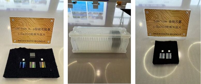
GaFuture Semiconductor Technology (Jinjiang) Co., Ltd. is founded based on the State Key Discipline Laboratory of Wide Bandgap Semiconductor Technology and the National Engineering Research Center for Wide Bandgap Semiconductors at Xidian University. The technical team has been deeply engaged in the epitaxial growth technology of Gallium Oxide semiconductors for over ten years, holding more than 30 authorized patents in areas such as Gallium Oxide epitaxy, defect control, doping simulation, and process optimization. The team has published over 60 academic papers and possesses fully domestic Gallium Oxide epitaxial equipment and complete process systems with independent intellectual property rights.
The company takes heterogeneous epitaxy and an AI-driven material design platform as its core technologies, addressing key industry challenges including the high cost of Gallium Oxide materials, the difficulty of p-type doping, and poor heat dissipation. It has established a complete industrial chain covering epitaxial equipment design and manufacturing, AI-guided material design, large-area high-quality epitaxial processing, as well as back-end device design and tape-out.