


Member News
【Member News】Qi Hongji, Chairman of Hangzhou Fujia Gallium Industry: How Far Is the Industrialization of Gallium Oxide?
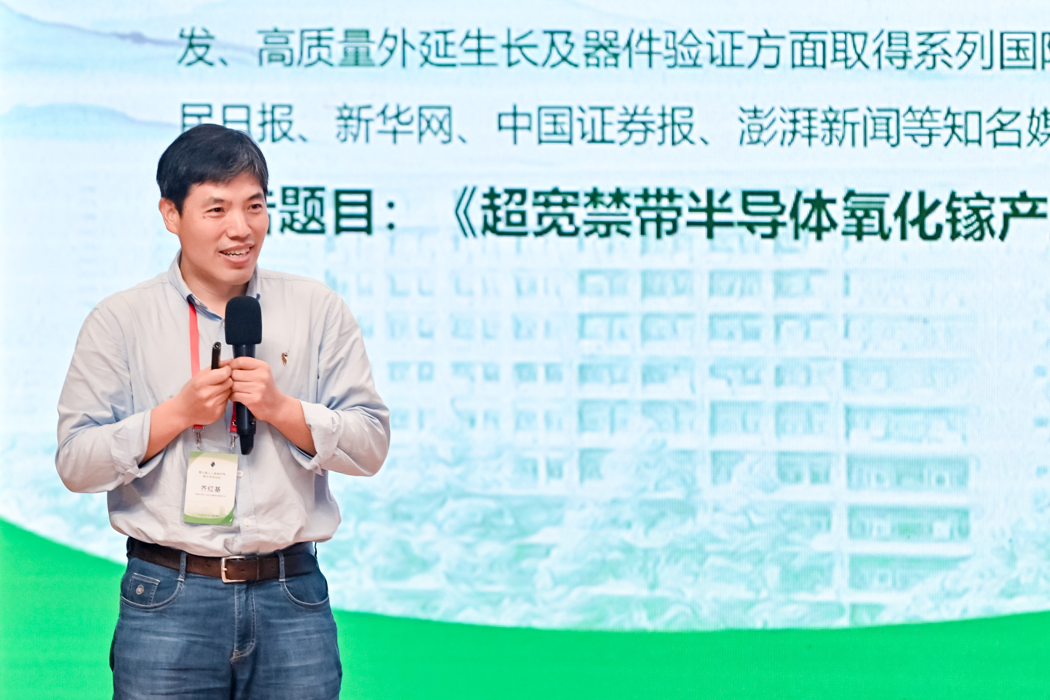
日期:2025-11-14阅读:443
To enhance the scientific research strength and technological level in the field of Synthetic Crystal and related areas, and further promote the development of Synthetic Crystal in China. The 5th Youth Conference on Synthetic Crystal Materials was held in Fuzhou, Fujian Province from November 7th to 9th, 2025. Qi Hongji, the chairman of Hangzhou Fujia Gallium Technology Co., LTD., (hereinafter referred to as Fujia Gallium), was invited to attend the conference and deliver a talk titled “How Far is the Industrialization of Ultra-Wide Bandgap Semiconductor Gallium Oxide?” as an invited speaker. The report provided a systematic analysis of the Gallium Oxide industry from multiple perspectives, including China’s resource endowment and energy policies, market demand for power semiconductors, the performance and cost advantages of Gallium Oxide materials, the stages of industrialization in the Gallium Oxide field, and the necessary work for advancing industrialization. Based on market demand, the report divides Gallium Oxide industrialization into four stages: awareness, utility, usability, and desire to use. Drawing on Fujia Gallium’s practical experience, it offered an in-depth analysis of the bottlenecks and strategies for overcoming them, which resonated widely and sparked lively discussion among the attendees.
Key Points
Demand side
1、China’s resource endowment—“abundant coal but scarce natural gas, with vast wind and solar potential”—together with rapidly increasing energy demand, determines the country’s unique energy policy: a strong emphasis on new energy development.
2、China’s new energy targets for 2030, 2040, 2050, and 2060 are driving explosive demand for power devices. Industrial infrastructure across sectors such as new energy vehicles, data centers, photovoltaic power generation, energy storage, and rail transit all require substantial support from high-performance semiconductor materials.
The Position of Gallium Oxide in Future Power Devices
1、Gallium Oxide, as a core material for ultra-wide bandgap semiconductors, offers high performance and low-cost advantages, making it well-suited to meet the rapidly growing demand in the future power semiconductor sector.
2、China’s abundant gallium reserves, combined with the massive downstream demand for power devices, position the country to take an international lead in the Gallium Oxide field.
3、Policy support—such as the directives from the Fourth Plenary Session of the 20th Central Committee of the Communist Party of China, Shanghai’s industrial layout, and the Ministry of Industry and Information Technology’s six major industrial directions emphasizing new materials and new energy—has accelerated the industrialization of Gallium Oxide.
Industrialization of Gallium Oxide
1、The industrialization of Gallium Oxide can be divided into four stages: existence, use, ease of use, and desire to use, covering the full chain of Gallium Oxide raw materials, single-crystal substrates, epitaxy, devices, and modules.
2、Once Gallium Oxide single crystals and epitaxial wafers exceed 6 inches, Gallium Oxide-based devices can accelerate iteration leveraging mature silicon power device fabrication lines.
3、In scaling up Gallium Oxide single-crystal substrates and epitaxial wafers, quality must be prioritized. Research on material defects and enhancement of epitaxial mobility is critical for rapid performance improvement of Gallium Oxide devices.
4、The preparation of Gallium Oxide substrates and epitaxial wafers should consider production efficiency. “One-click crystal growth” equipment and MOCVD epitaxy provide a foundation for future batch production.
5、The first domestic production line with an annual output of 10,000 6-inch Gallium Oxide substrates and epitaxial wafers will ensure material supply for the commercialization of Gallium Oxide devices in China.
6、During Gallium Oxide R&D and industrialization, the application of artificial intelligence will accelerate material performance iteration. China’s AI-driven crystal growth patent layout in mainstream international Gallium Oxide technology routes (EFG and VB) will provide a competitive advantage in future global markets.
7、China’s leading position in MOCVD epitaxy will significantly shorten the timeline for introducing Gallium Oxide power devices to the market.
8、Breakthroughs in MBE epitaxial wafer technology have been validated by downstream customers, achieving domestic substitution and performance improvement, effectively mitigating the impact of Japan’s embargo on these products since 2022.
9、The low thermal conductivity of Gallium Oxide has already found preliminary engineering solutions. Heat dissipation in power devices is an engineering challenge, not a fundamental obstacle to industrialization.
10、High-quality P-type films produced by MOCVD epitaxy represent a key technical pathway for P-type layers in future Gallium Oxide devices. Currently, research focuses on PN junction verification and device validation, with performance of P-type Gallium Oxide films nearly meeting device requirements.
11、Research on device reliability is receiving increasing attention, providing essential support for safe practical applications.
12、The domestic and international industrialization of Gallium Oxide has progressed rapidly from early existence to practical utility. The high homogeneity of melt growth and MOCVD technology will significantly accelerate the advancement of large-size substrates and epitaxial wafers.
13、Abundant silicon-based power device lines, both domestic and international, provide wafer fabrication support for low-cost Gallium Oxide device production, further expediting industrialization.
The rapid industrial application of Gallium Oxide devices is an inevitable trend. The rapid iteration of devices and application scenarios is the core factor determining industrial application. The defect of Gallium Oxide materials, P-type Gallium Oxide materials, and the heat dissipation and reliability of Gallium Oxide devices are important research topics for the future industrialization of devices. It is necessary for colleagues in the Gallium Oxide field to join hands to tackle these problems and achieve the goal of "enabling the world to use good materials" as soon as possible.
Product Introduction
Gallium Oxide Equipment:
The company has developed the world’s first “One-Click Crystal Growth” EFG (Edge-defined Film-fed Growth) system, capable of growing 2–6-inch crystals. Currently, it holds 6 domestic patents and 4 international patents and can provide the equipment along with a complete process package.
The company independently developed a fully automatic VB (Bridgman) crystal growth system and was the first in China to overcome the technical bottleneck of 6-inch single crystal growth, achieving large-size VB single crystal preparation. It currently holds 6 domestic patents and 4 international patents, and VB equipment and process packages can be provided according to customer requirements.
Taking into account the brittleness and cleavage characteristics of Gallium Oxide, the company has developed 2–6-inch Gallium Oxide single crystal substrate grinding and polishing equipment. Mature grinding, polishing, and cleaning process packages are available to customers as needed.
Gallium Oxide Single Crystal Substrates:
As one of China’s earliest pioneers in Gallium Oxide single crystal growth research and a leading industry supplier, we are committed to providing global customers with high-quality Gallium Oxide single crystal substrates. Our product line includes 26 standard Gallium Oxide substrate products, covering sizes of 5×5.5 mm, 10×10.5 mm, and 2–6 inches. We also offer various sizes (e.g., 10×15 mm, 20×20 mm) and customizable electrical properties and crystal orientations (e.g., (100), (010), (001)) to meet the needs of high-quality epitaxial wafer development and mass production.
Gallium Oxide Epitaxial Wafers:
Based on mature MOCVD (Metal-Organic Chemical Vapor Deposition) and MBE (Molecular Beam Epitaxy) platforms, our product line includes 15 standard Gallium Oxide epitaxial wafer products (sizes 10×10.5 mm, 2–6 inches) and customized 10×15 mm MBE Ga2O3 epitaxial wafers, providing customers with integrated “substrate-to-epitaxy” solutions. The epitaxial growth process uses precise process control systems, allowing customization of key parameters suc h as epitaxial layer thickness, doping concentration, and compositional uniformity according to customer requirements, supporting the development and production of devices across different power levels and functional types.
About Fujia Gallium
Hangzhou Fujia Gallium Technology Co., LTD., founded on December 31, 2019, is the first "hard technology" enterprise registered by Hangzhou Institute of Optics and Fine Mechanics. With the vision of "Making the World Use Good Materials", the company focuses on the industrialization work of wide bandgap semiconductor Gallium Oxide materials. The core products include Gallium Oxide single crystal substrates, MOCVD epitaxial wafers, MBE epitaxial wafers, The VB method and EFG method crystal growth equipment, substrate grinding and polishing equipment, etc. provide systematic solutions for material development, accelerate the full chain connection of the ultra-wide bandgap Gallium Oxide industry, and promote the application of Gallium Oxide materials in power devices, microwave and radio frequency devices, and optoelectronic detection fields.The company's series of important achievements in the development of Gallium Oxide have been featured and reported by well-known media such as People's Daily, Xinhuanet, China Securities News, and The Paper.
Corporate Honors:
In 2022, it won the Zhejiang Province Science and Technology Small and Medium-Sized Enterprise; National High-Tech Enterprise in 2023; In 2024, it will be awarded as Hangzhou Enterprise High-Tech Research and Development Center and Zhejiang Special Small and Medium-Sized Enterprise. Obtain ISO9001 quality system certification in 2025 (No. 20225Q20294R0M) and 2024 Hangzhou “Rising Eagle” Enterprise. In the field of Gallium Oxide, the company is leading the drafting of China’s first national standard and has undertaken projects from the National Development and Reform Commission and the Ministry of Industry and Information Technology. It undertook one Gallium Oxide project for the National Development and Reform Commission and participated in three national and provincial projects from the Ministry of Science and Technology, Zhejiang Province, and Shanghai. In addition, it has obtained 12 international patents authorized (6 in the United States and 6 in Japan), 40 domestic patents authorized, 3 trademark certification and registration of "Fujia Gallium", and 4 software copyrights (crystal growth control software of "one-click crystal growth").
