Paper Sharing
【Member Papers】Multi-fin normally-off β-Ga₂O₃ vertical transistor with a breakdown voltage exceeding 10 kV
日期:2025-10-09阅读:538
Researchers from the Novel Crystal Technology have published a dissertation titled "Multi-fin normally-off β-Ga2O3 vertical transistor with a breakdown voltage exceeding 10 kV" in Applied Physics Express.
Background
β-Ga₂O₃ has attracted significant attention in power electronics, particularly for electric vehicles, power conditioning, and high-voltage switching applications, due to its large bandgap (4.5–4.9 eV), high theoretical breakdown field (6–8 MV/cm), and excellent Baliga’s figure of merit. Both lateral and vertical transistors have been developed; however, high-voltage vertical transistors face fabrication challenges, requiring high-quality, low-donor-concentration (≤5×10¹⁵ cm⁻³), thick epitaxial layers (≥50 µm), and effective edge-termination structures, with Cl incorporation being problematic in (001)-oriented layers. Recently, low-donor-concentration thick epitaxial layers have been achieved on (011) substrates, enabling the fabrication of high-voltage vertical transistors. In this work, multi-fin β-Ga₂O₃ vertical transistors were fabricated on such (011) epitaxial wafers, exhibiting normally-off behavior and a breakdown voltage exceeding 10 kV, demonstrating the potential of β-Ga₂O₃ vertical power devices for ultra-high-voltage applications.
Abstract
We demonstrated a multi-fin normally-off β-Ga2O3 vertical transistor with a breakdown voltage exceeding 10 kV, specific on-resistance of 289 mΩ·cm2, and power figure-of-merit of 0.35 GW/cm2. The vertical transistor was fabricated on a low-donor-concentration (Nd-Na≈ 1.8×1015 cm-3) and thick (thickness≈ 85 µm) epitaxial layer grown on a (011) β-Ga2O3 substrate by halide vapor phase epitaxy to enhance the breakdown voltage. The breakdown voltage exceeding 10 kV is the highest reported for β-Ga2O3 vertical transistors. This result indicates the great potential of Ga2O3 vertical power devices.
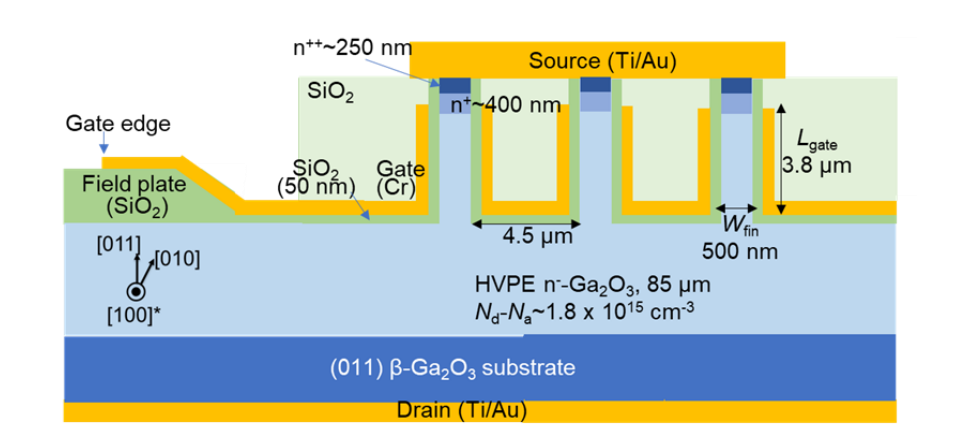
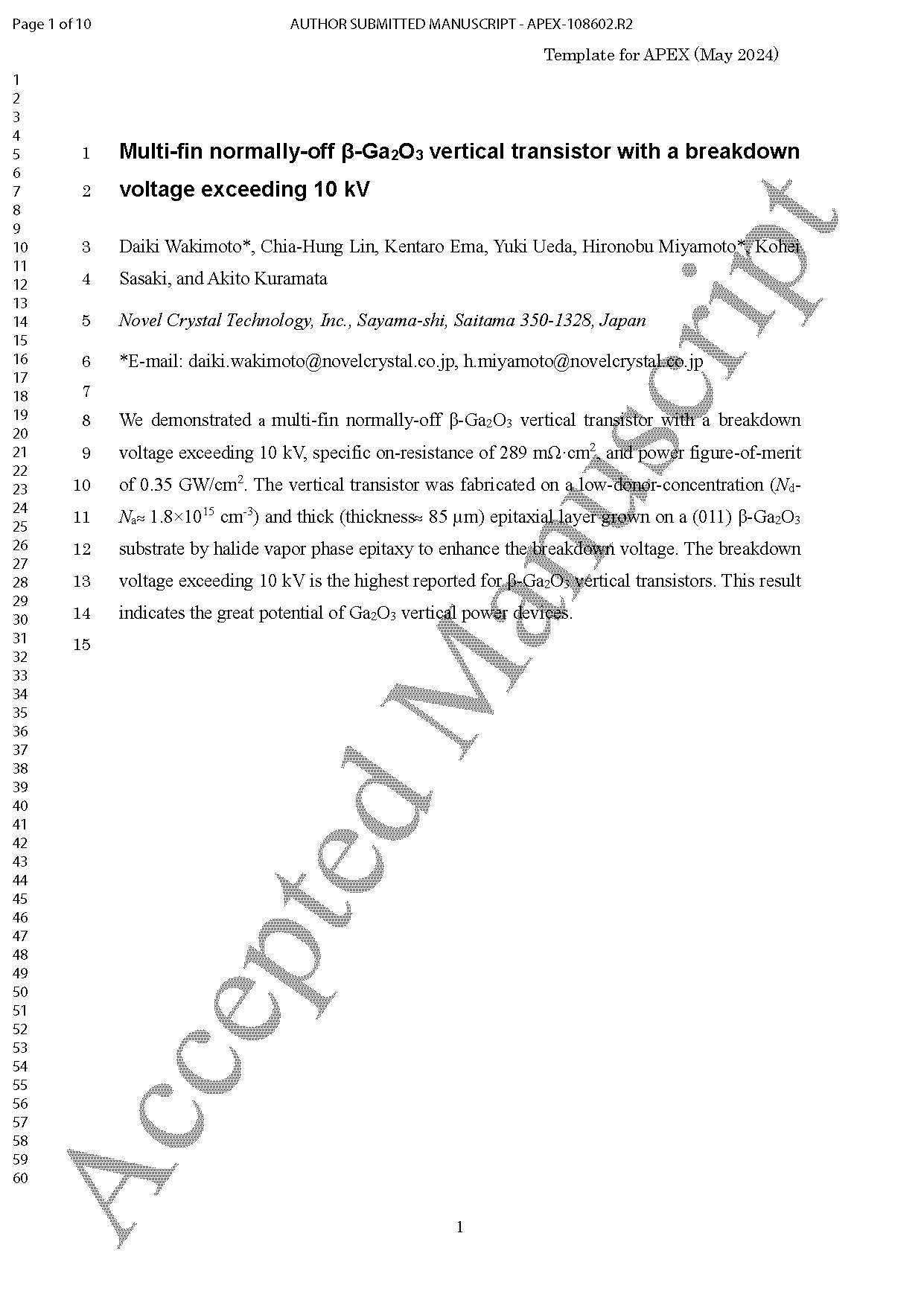
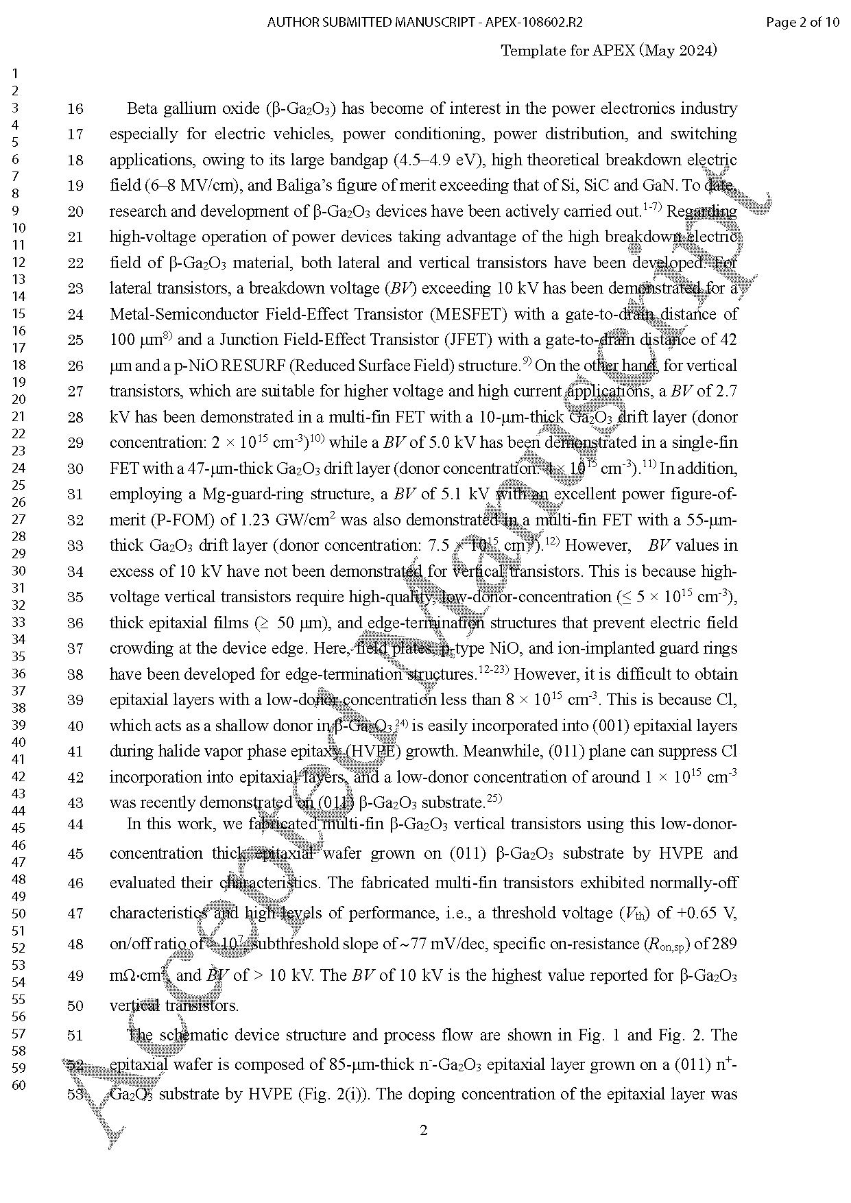
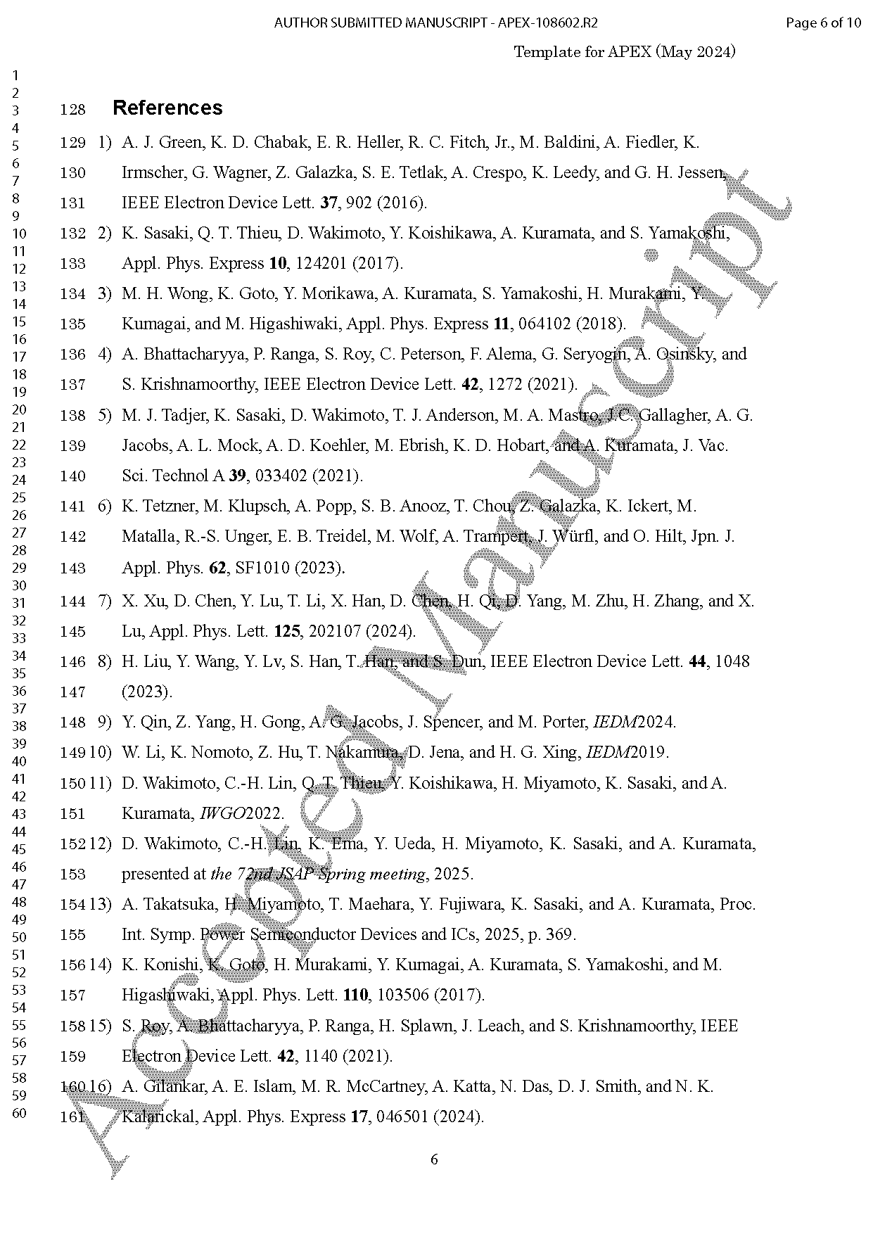
Fig. 1. Schematic cross-section of a multi-fin β-Ga2O3 vertical transistor with a gate field plate.
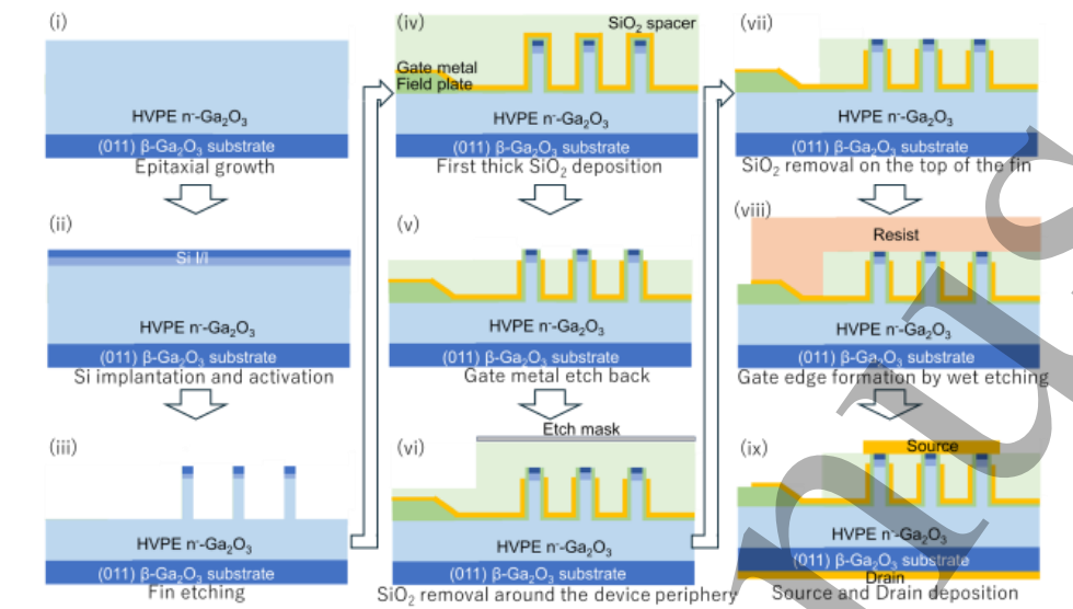
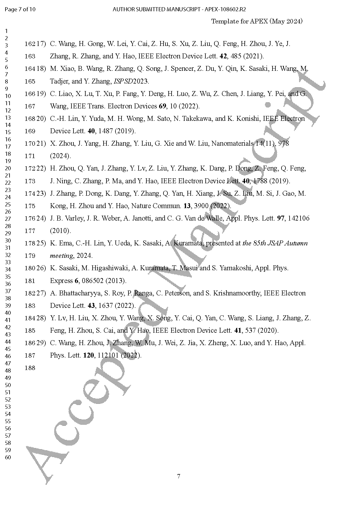
Fig. 2. Schematic cross-section of a multi-fin β-Ga2O3 vertical transistor fabrication process flow.
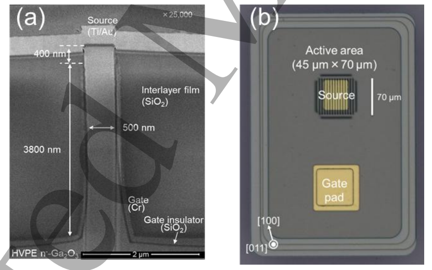
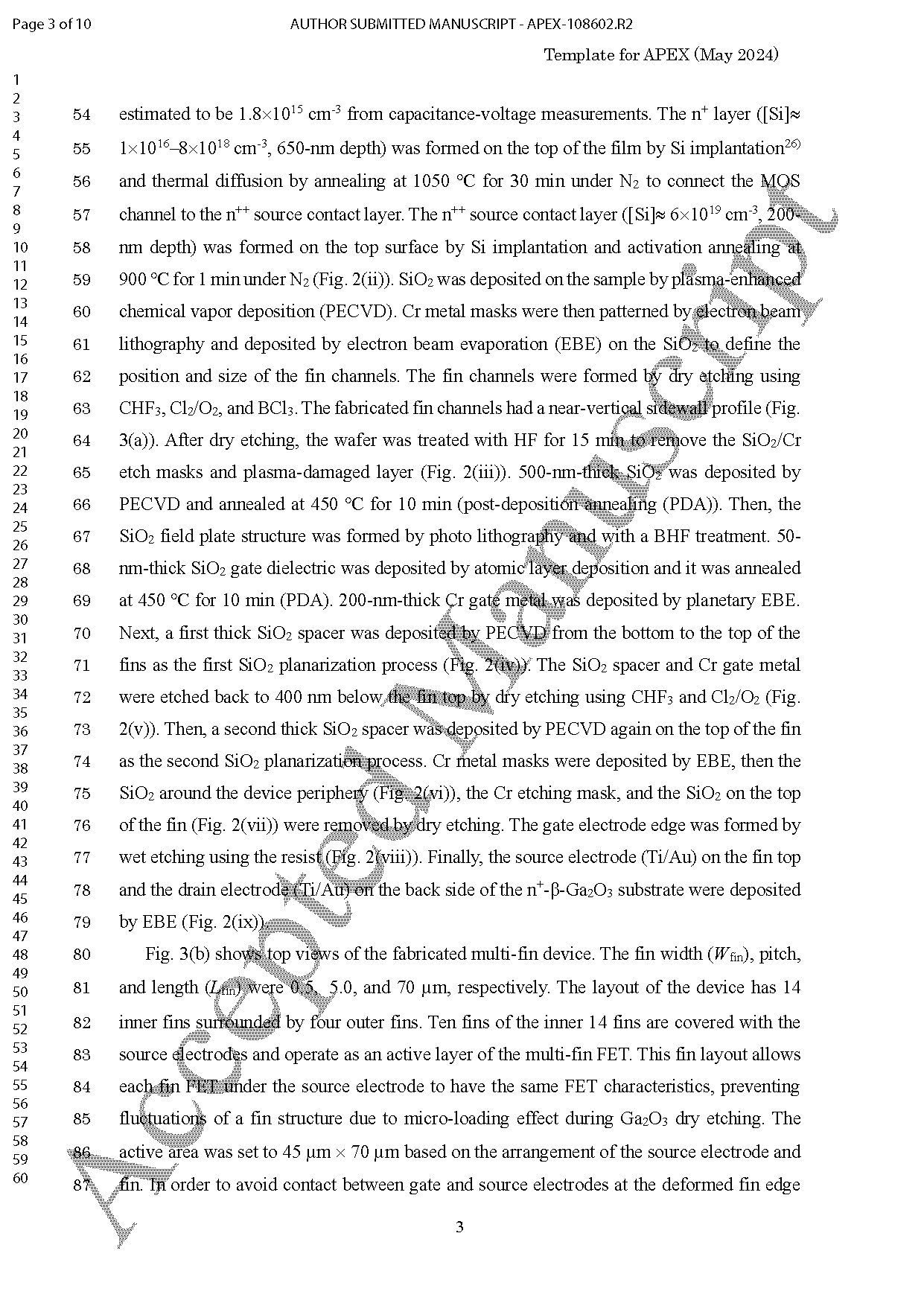
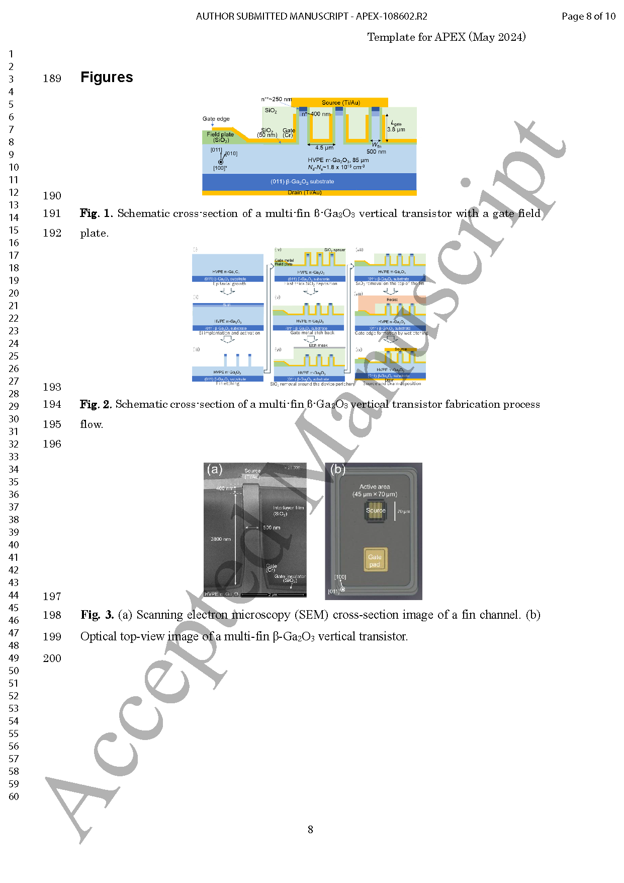
Fig. 3. (a) Scanning electron microscopy (SEM) cross-section image of a fin channel. (b) Optical top-view image of a multi-fin β-Ga2O3 vertical transistor.
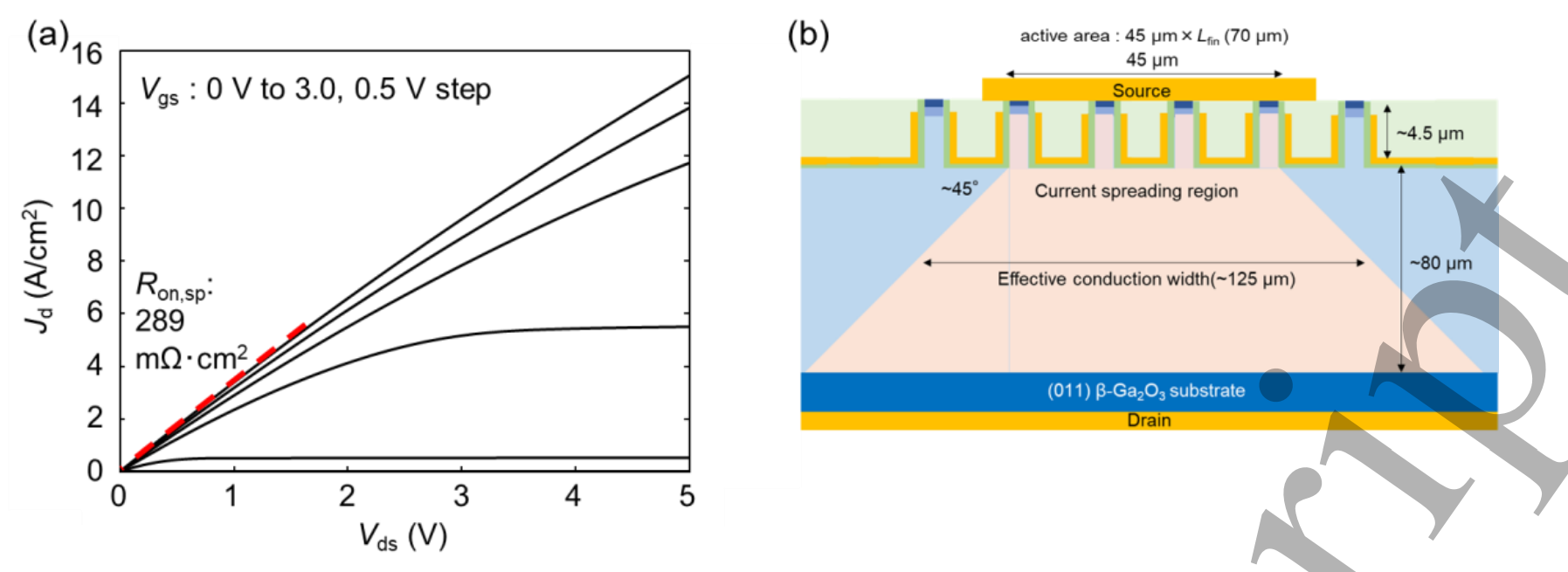
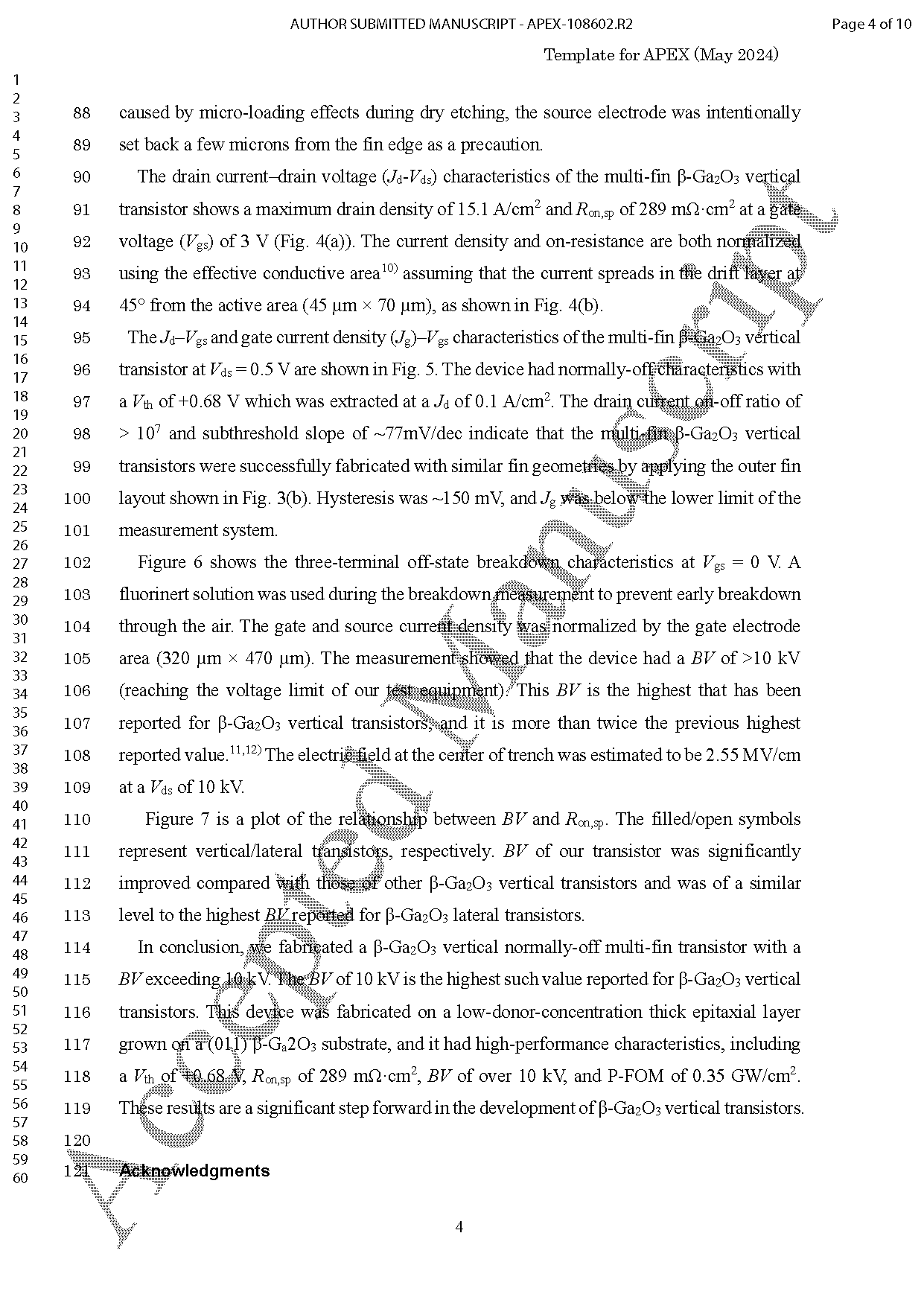
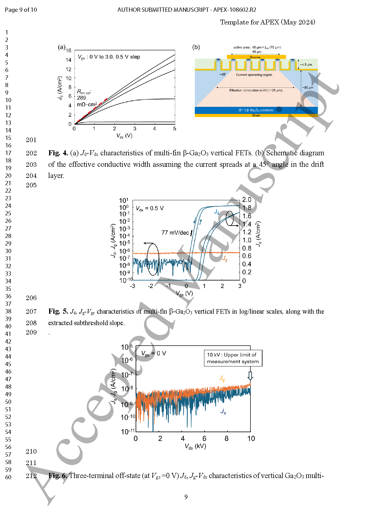
Fig. 4. (a) Jd-Vds characteristics of multi-fin β-Ga2O3 vertical FETs. (b) Schematic diagram of the effective conductive width assuming the current spreads at a 45° angle in the drift layer.
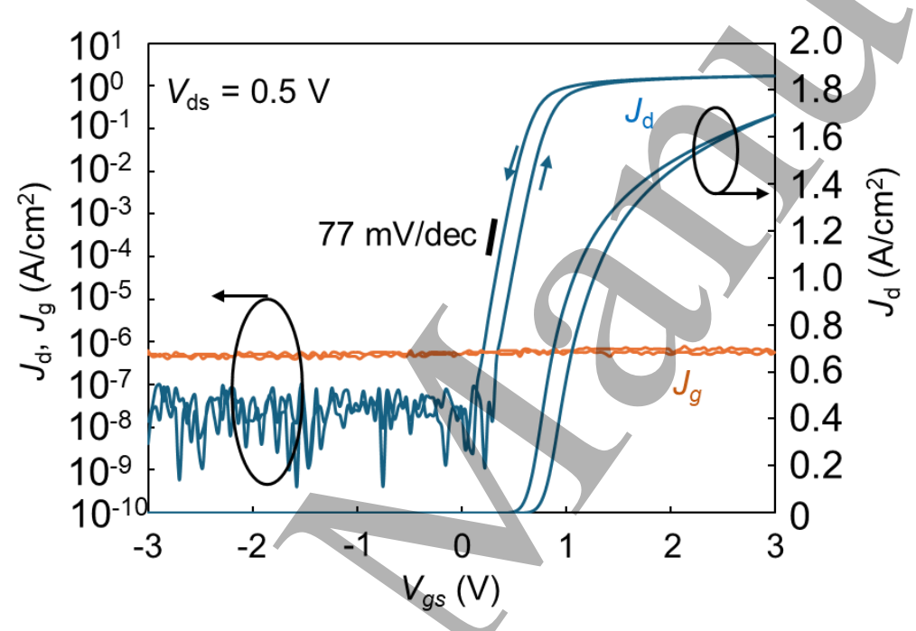
Fig. 5. Jd, Jg-Vgs characteristics of multi-fin β-Ga2O3 vertical FETs in log/linear scales, along with the extracted subthreshold slope.
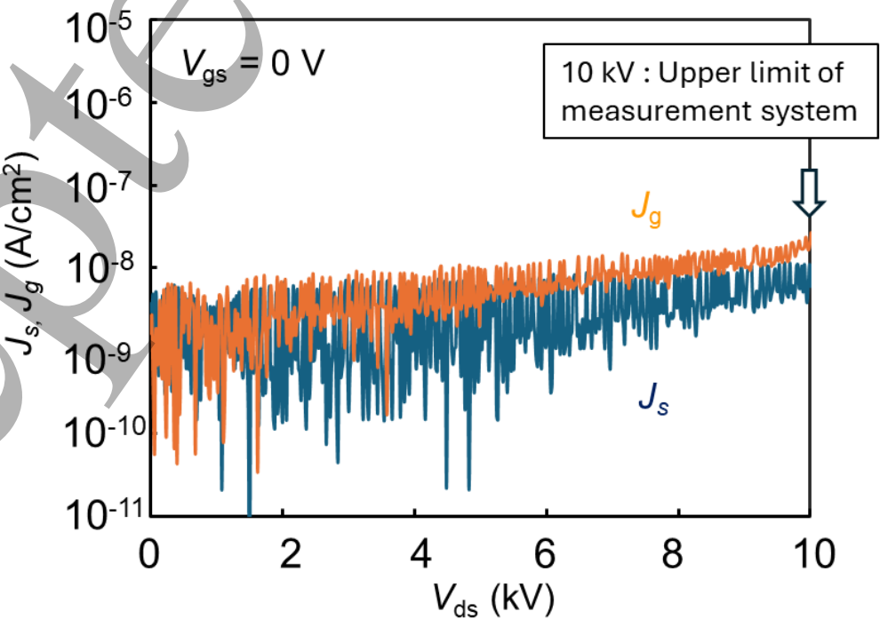
Fig. 6. Three-terminal off-state (at Vgs =0 V) Jd, Jg-Vds characteristics of vertical Ga2O3 multi-finFETs.
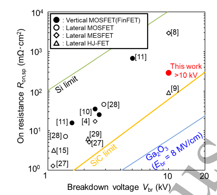
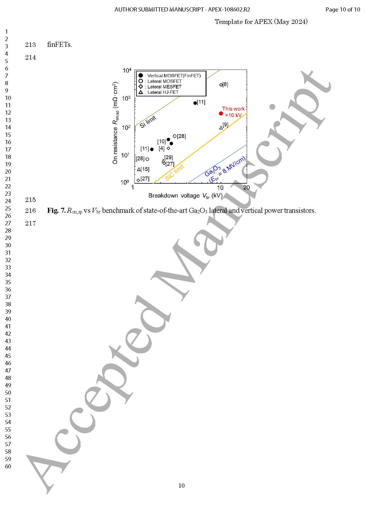
Fig. 7. Ron,sp vs Vbr benchmark of state-of-the-art Ga2O3 lateral and vertical power transistors.
DOI:
doi.org/10.35848/1882-0786/ae0d2a