Paper Sharing
【Member Papers】Anisotropic Ga₂O₃ Nanograting with Photonic and Band Engineering Enables High-Sensitivity Solar-Blind Photodetectors
日期:2025-10-09阅读:561
Researchers from the Beijing University of Posts and Telecommunications and Nanjing University of Posts and and Telecommunications published a dissertation titled " Anisotropic Ga2O3 Nanograting with Photonic and Band Engineering Enables High-Sensitivity Solar-Blind Photodetectors" in Advanced Optical Materials.
Project Support
This work was supported by the National Key Research and Development Program of China(Grant2022YFB3605404), the Natural Science Re search Start-up Foundation of Recruiting Talents of Nanjing University of Posts and Telecommunications (Grant XK1180924052), the Natural Science Foundation of Jiangsu Province (Grant No. BK20250657), the China Scholarship Council program (Grant 202406470087), and the BUPT Excel lent Ph.D. Students Foundation (Grant CX20242038).
Background
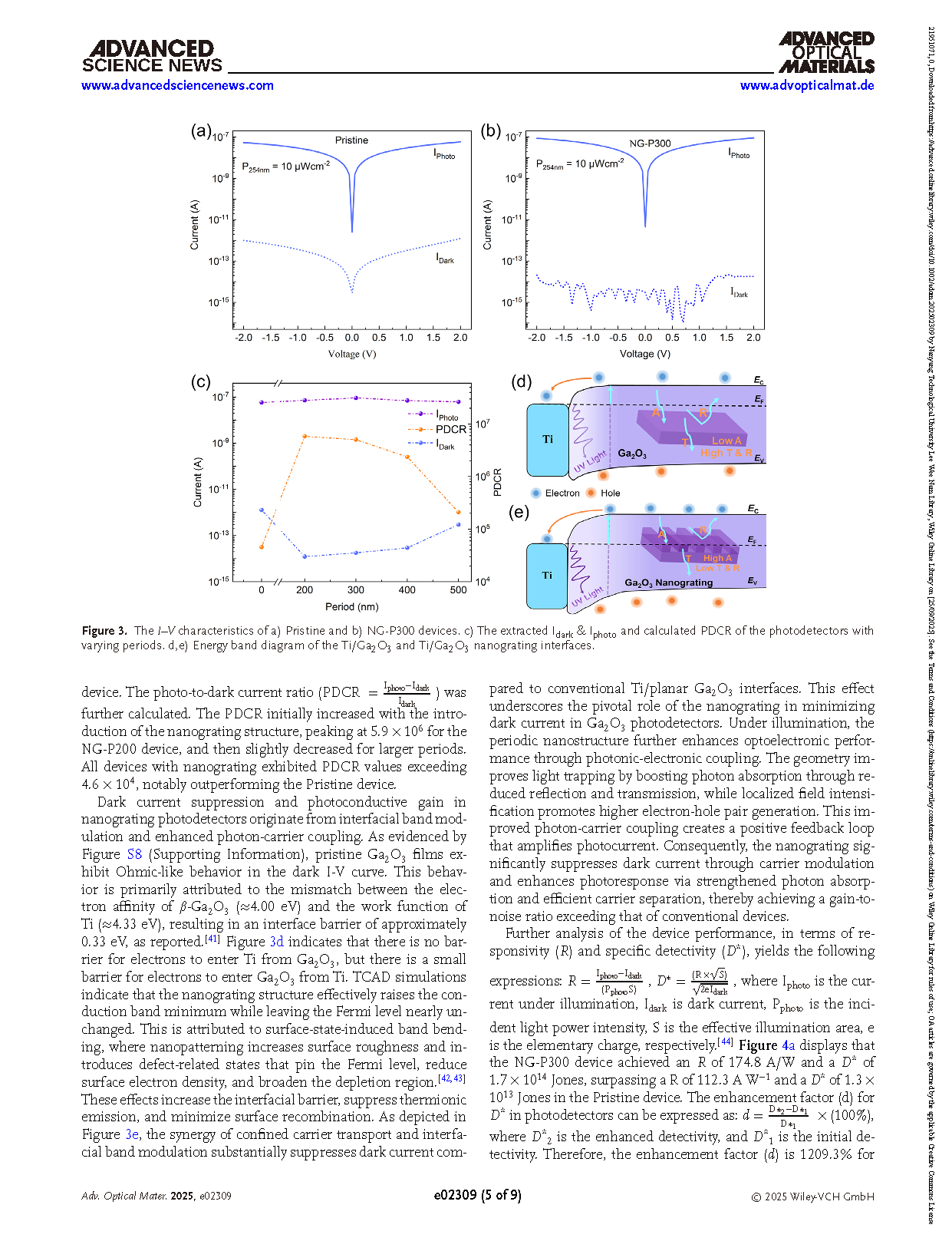
Solar-blind ultraviolet (200–280 nm) photodetectors are critical for applications such as secure communication, environmental monitoring, and space-based detection. Ga2O3, with its ultra-wide bandgap, intrinsic solar-blind absorption, and high radiation tolerance, is an ideal material, but devices are still limited by surface-defect-induced dark current, low light absorption efficiency, and weak polarization sensitivity. Nanostructure engineering, particularly one-dimensional nanograting photonic crystals, can enhance light absorption while modulating carrier transport and polarization response, offering a promising route for high-performance Ga2O3 SBPDs. A deeper understanding of metal–nanostructure interface effects on energy bands and photocarrier dynamics is still needed to guide device optimization.
Abstract
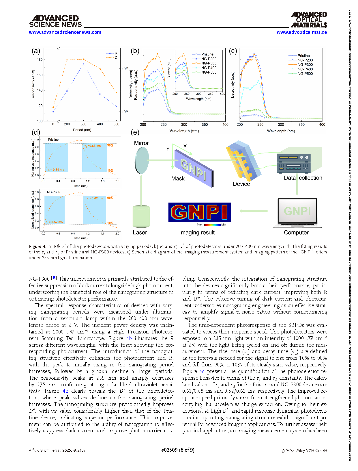
Ga2O3-based solar-blind UV photodetectors exhibit intrinsic solar-blind absorption and radiation tolerance but remain limited by surface leakage current, inefficient photon-carrier coupling, and weak polarization sensitivity. Herein, a nanograting photonic structure is introduced to modulate carrier dynamics through photonic and band engineering. This design strengthens photon-carrier coupling and tunes interfacial energy band structure to enhance photoconductive gain and suppress dark current. Nanograting structure effectively reduces dark current through an upshifted interfacial conduction band, while simultaneously intensifying light absorption via reduced reflectance and transmittance. Its inherent anisotropy enables polarization discrimination without external optics or phase tuning approaches. The optimized device achieves an ultra-low dark current of 1.8 × 10⁻¹⁴ A, a responsivity of 174.8 A W−1, a specific detectivity of 1.7 × 10¹⁴ Jones (a 1209.3% improvement), and a high polarization ratio of 570%, remarkably surpassing planar Ga2O3 solar-blind photodetectors (SBPDs). This work demonstrates a novel strategy through photonic-electronic integration for high-sensitivity, low-noise SBPDs with excellent polarization response.
Conclusion
In conclusion, the mechanisms underlying enhanced light–matter interactions and carrier transport dynamics in nanograting-engineered Ga₂O₃ photodetectors were demonstrated. This strategy effectively resolves the trade-off between responsivity and dark current through interfacial barrier modulation and nanostructure–enabled light management. The dark current was reduced to an ultra-low level of 1.8 × 10⁻¹⁴ A by raising the contact barrier. The nanograting simultaneously increases light absorption by lowering reflectance and transmittance, thereby improving the photoresponse. Moreover, the intrinsic anisotropy enables efficient polarization discrimination without relying on external optics or phase-tuning techniques. The device thus achieves outstanding performance, with a specific detectivity of 1.7 × 10¹⁴ Jones, a responsivity of 174.8 A W⁻¹, a markedly augmented PDCR, and high-resolution polarization sensitivity, reflecting improved device functionality. This work bridges photonics design principles with wide-bandgap semiconductor electronics, laying the foundation for next-generation optoelectronic systems and future applications.
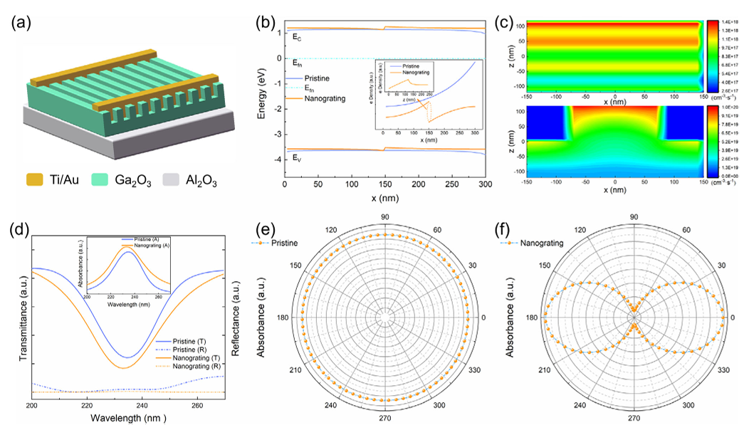
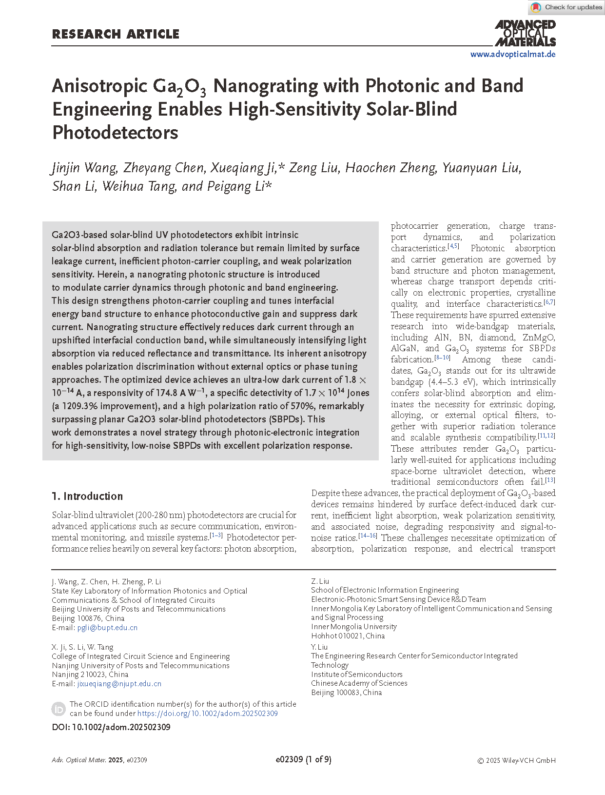
Figure1. a) Schematic diagram of the photo detector with Ga2O3 nano grating. b) Simulated energy band structure diagram. The inset shows the extracted lateral electron distribution. c) Optical growth rate, d) reflectivity, transmittance, and absorbance, e,f) absorbance versus polarization angle for Ga2O3 films and Ga2O3 nanograting.

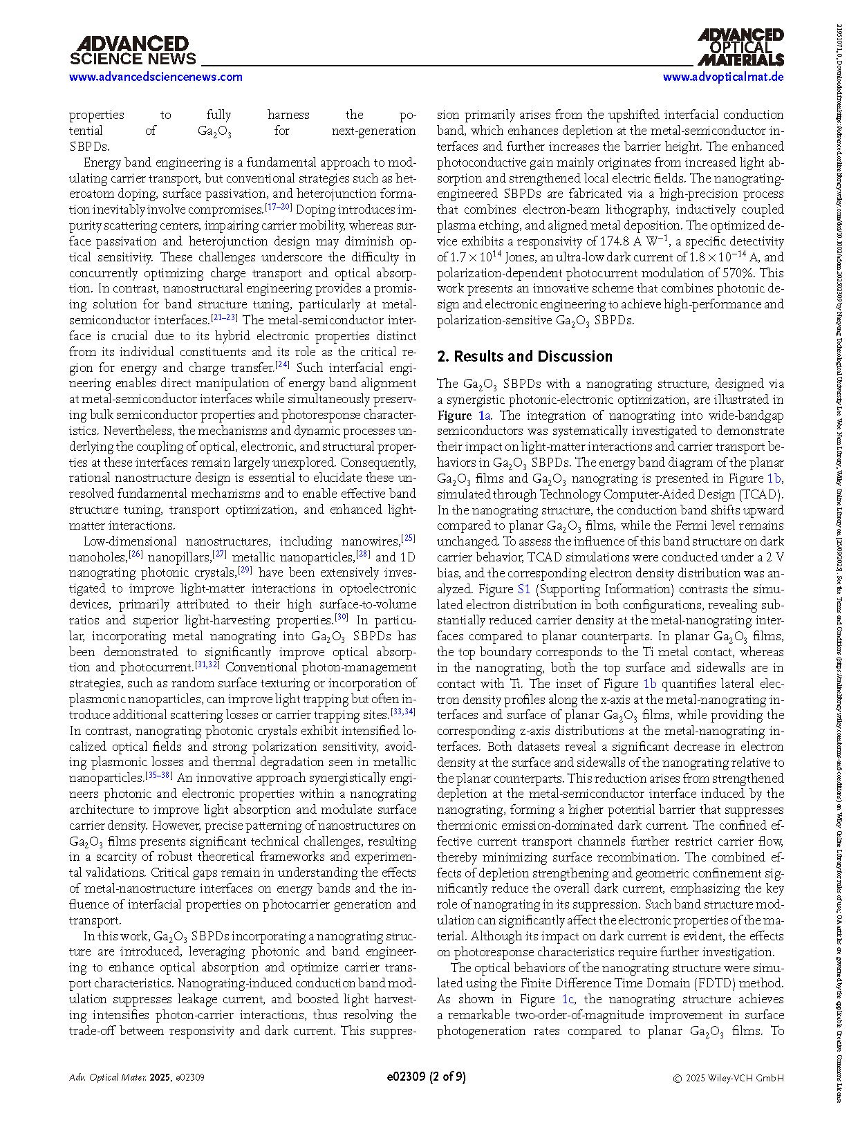
Figure 2. a) XRD pattern of the β-Ga2O3 films. b) The rocking curves of (-201) diffraction peak. c) The HRTEM image of β-Ga2O3 films. d) The atomic arrangement of β-Ga2O3 (-201) planes. e) Planar and f) cross-sectional SEM images of the Ga2O3 nanograting. g,h) UV absorbance spectrum of Ga2O3 films and Ga2O3 nanograting.
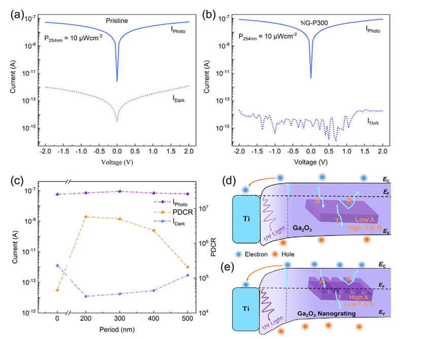
Figure 3. The I–V characteristics of a) Pristine and b) NG-P300 devices. c) The extracted Idark &Iphoto and calculated PDCR of the photodetectors with varying periods. d,e) Energy band diagram of the Ti/Ga2O3 and Ti/Ga2O3 nanograting interfaces.
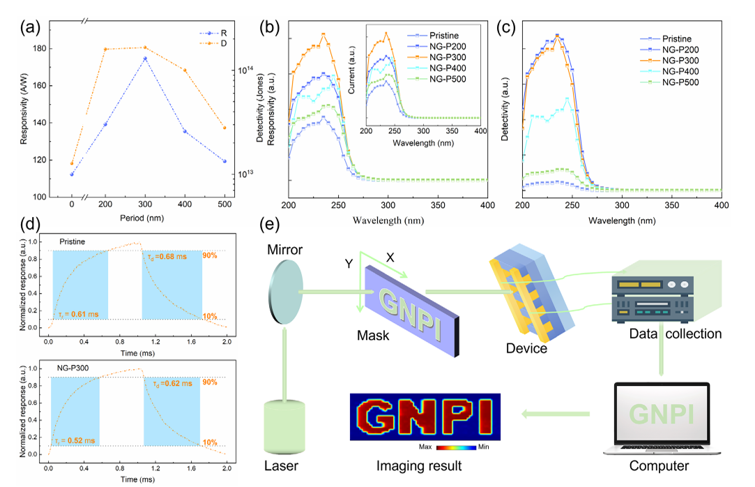
Figure 4. a) R&D* of the photodetectors with varying periods. b) R, and c) D* of photodetectors under 200–400 nm wavelength. d) The fitting results of the τr and τd of Pristine and NG-P300 devices. e) Schematic diagram of the imaging measurement system and imaging pattern of the “GNPI” letters under 255 nm light illumination.
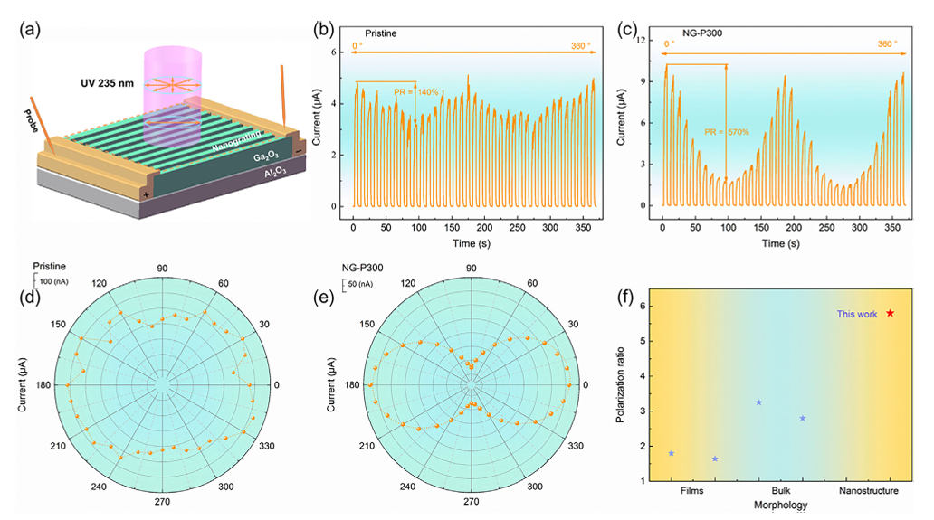
Figure 5. a) Schematic diagram of the polarization-sensitive device. b,c) Time-resolved photocurrent response under polarization light. d,e) Diagram of photocurrent versus polarization angle of devices. f) Comparison of PR across different polarization photodetectors based on various Ga2O3 morphologies.
DOI:
doi.org/10.1002/adom.202502309