Paper Sharing
【Domestic Papers】UV-promoted surface-enhanced Raman spectroscopy via heterojunction of few-layer MoS₂ flakes on acceptor-rich β-Ga₂O₃ microstrips
日期:2025-09-23阅读:429
Researchers from the Beijing University Of Technology have published a dissertation titled "UV-promoted surface-enhanced Raman spectroscopy via heterojunction of few-layer MoS2 flakes on acceptor-rich β-Ga2O3 microstrips" in Discover Nano.
Project Support
This research supported by the National Natural Science Foundation of China (Grant No.: 12374337), Beijing Natural Science Foundation (L241062), and Beijing Nova Program (20230484468).
Background
Surface-enhanced Raman spectroscopy (SERS) has attracted tremendous interest for ultrasensitive molecular detection with applications in chemical sensing, biomedical diagnostics, and environmental monitoring. Conventional electromagnetic enhancement using metallic nanostructures suffers from uniformity and cost issues, motivating the development of semiconductor-based chemical enhancement via charge-transfer (CT) processes. Two-dimensional transition metal dichalcogenides (2D-TMDs), with their stability, tunable bandgaps, and biocompatibility, have emerged as promising SERS substrates, with performance improvements achieved through defect engineering, alloying, and heterojunction strategies. Metal oxides, owing to their abundant defect states, also play a key role in CT-driven SERS enhancement. Combining 2D-TMDs with oxides has proven effective in boosting CT efficiency and sensitivity. β-Ga2O3, an ultra-wide bandgap semiconductor, offers high transparency and defect-rich states capable of facilitating CT under UV excitation. In this work, a novel heterojunction SERS substrate consisting of few-layer MoS2 and acceptor-rich β-Ga2O3 microstrips is proposed. For the first time, UV-activated CT processes from deep defect states in β-Ga2O3 to MoS2 were experimentally demonstrated, opening new opportunities for designing highly sensitive semiconductor-based SERS platforms.
Abstract
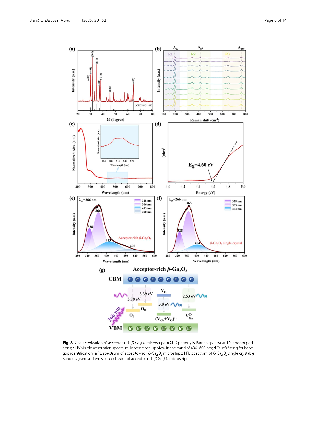
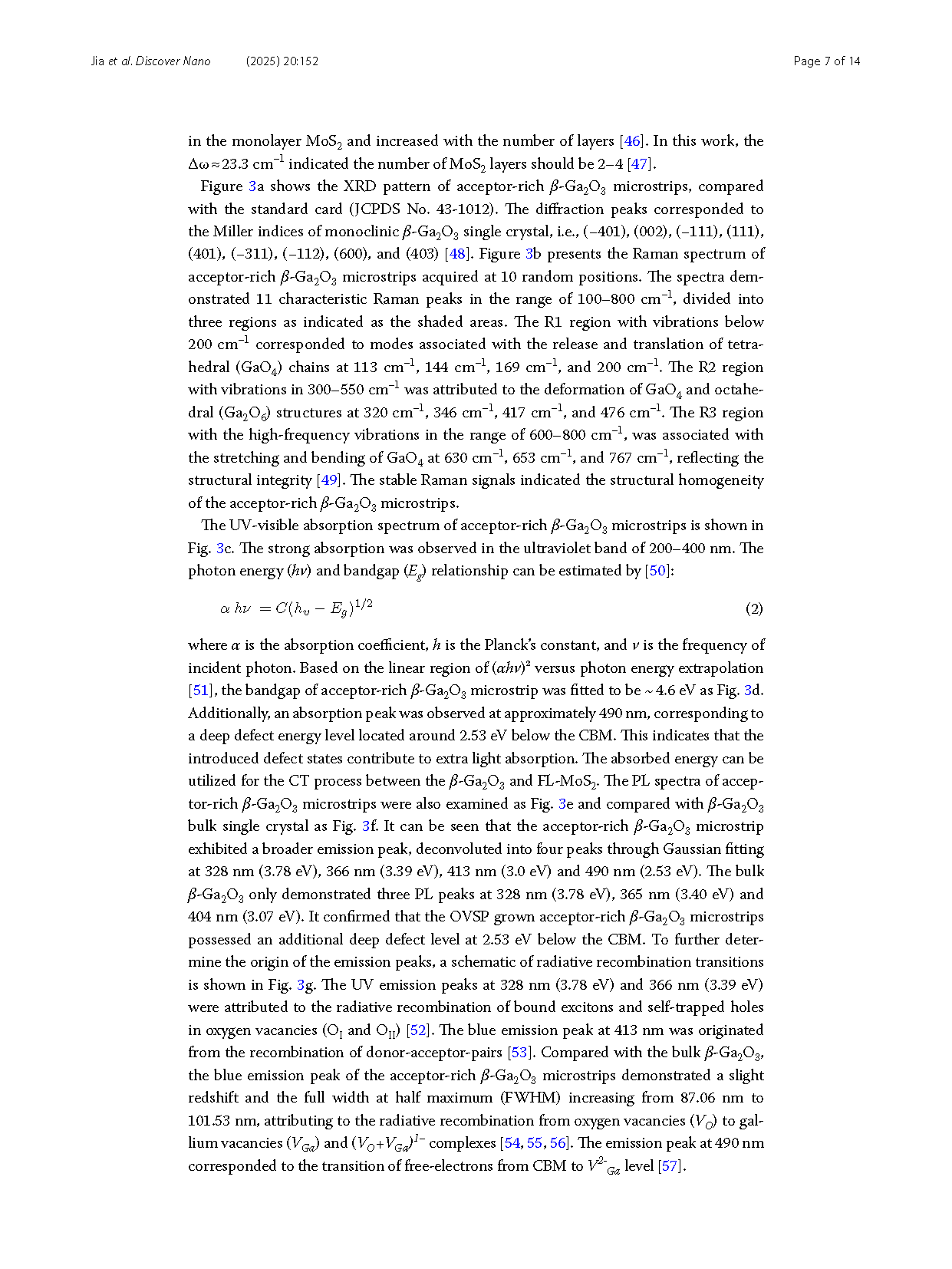
Surface-enhanced Raman spectroscopy (SERS) by 2D semiconductors relies on chemical (CM) enhancement driven by charge-transfer (CT) processes in bandgap alignment between molecules and substrates. Unfortunately, the low light absorption and weak conferment in the atomic-layer material limit the enhancement factor of Raman intensity (EFRI). Improving the utilization efficiency of excitation light is therefore essential for promoting SERS performance of 2D semiconductors. Here we develop a heterojunction SERS substrate, composed of few-layer MoS2 (FL-MoS2) flakes capping onto the acceptor-rich β-Ga2O3 microstrips grown by optical vapor supersaturated precipitation (OVSP). The acceptor-rich β-Ga2O3 microstrips excited by ultraviolet (UV) irradiation boost the CT processes between FL-MoS2 and analyte molecules, by which the EFRI was increased by two orders of magnitude up to 9.33 × 10⁴ with the limit of detection (LoD) down to 10⁻9 M for methylene blue (MB). The in-situ experiment unveils that the SERS improvement is originated from the photoinduced carries trapped by the deep acceptor of Ga2− vacancies (VGa2−) at 2.53 eV below conduction band minimum to facilitate the CT resonance. The present work provides new insights into the role of defect states in the chemical SERS mechanism, demonstrating the improvement of 2D-material substrate performance for ultrasensitive Raman detection.
Conclusion
In this work, a novel FL-MoS2@β-Ga2O3 heterojunction SERS substrate, composed of FL-MoS2 flakes covering onto the acceptor-rich β-Ga2O3 microstrips, was proposed. The OVSP-grown acceptor-rich β-Ga2O3 microstrips possessed massive V2-Ga deep detects, facilitating the multiple resonances including molecule resonance, exciton resonance, CT resonances, and FRET under UV excitation for giant Raman enhancement. The maximum EFRI up to 9.33 × 10⁴ was achieved for MB molecules adsorbed onto the FL-MoS2@β-Ga2O3, by which all above resonance processes were boosted by abundant free-electrons injection from the V2-Ga level at 2.53 eV below the CBM. The LoD was therefore reduced by two orders of magnitude to 10⁻9 M under UV activation. This study provides new insights into the role of defect states in 2D-TMDCs/oxide-semiconductor heterojunctions for CM enhancement, opening opportunities to design new plasmonic-free SERS substrates or further integrate with metal plasmonic nanostructures for efficient ultrasensitive Raman detection in future.
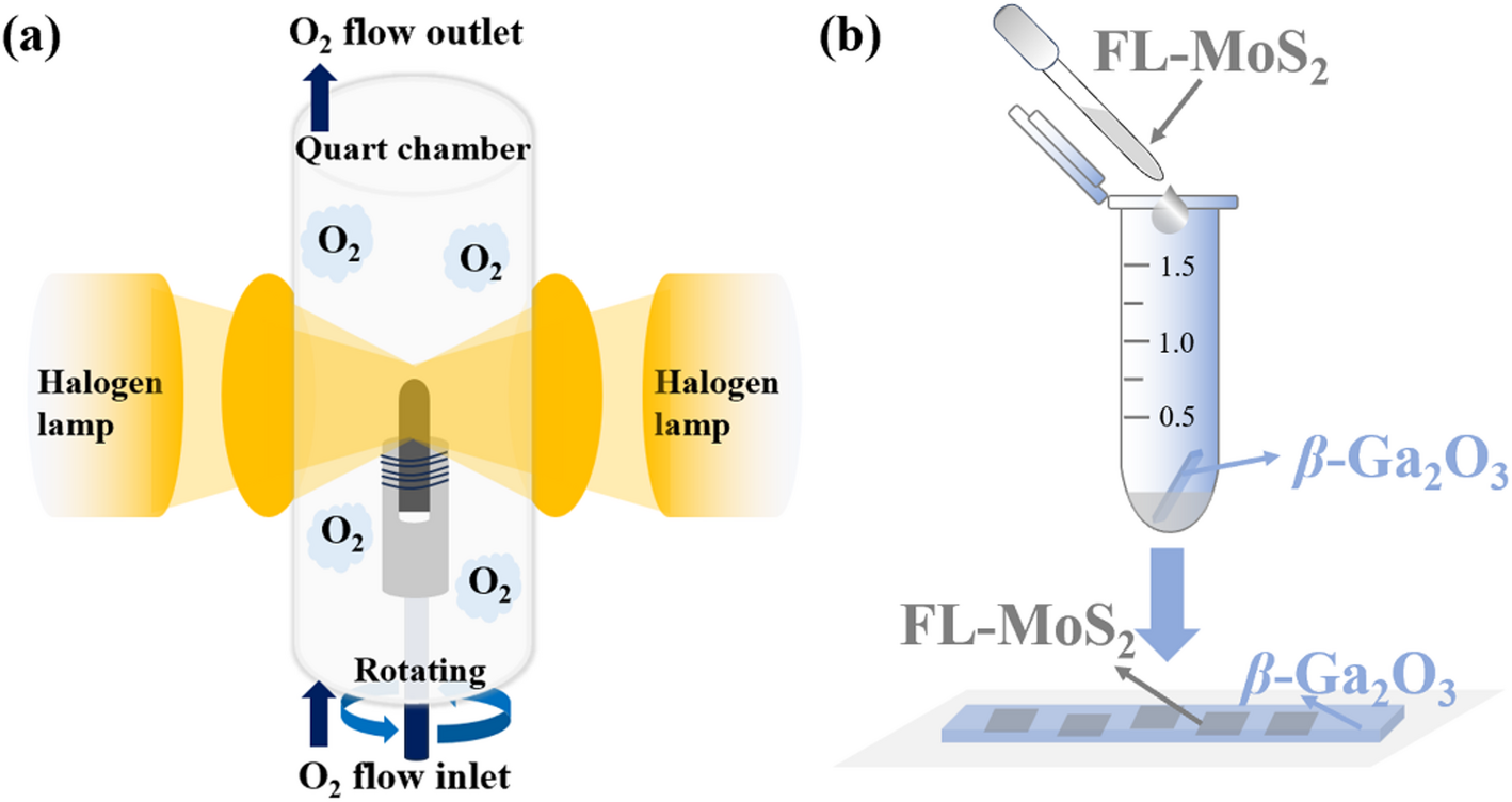
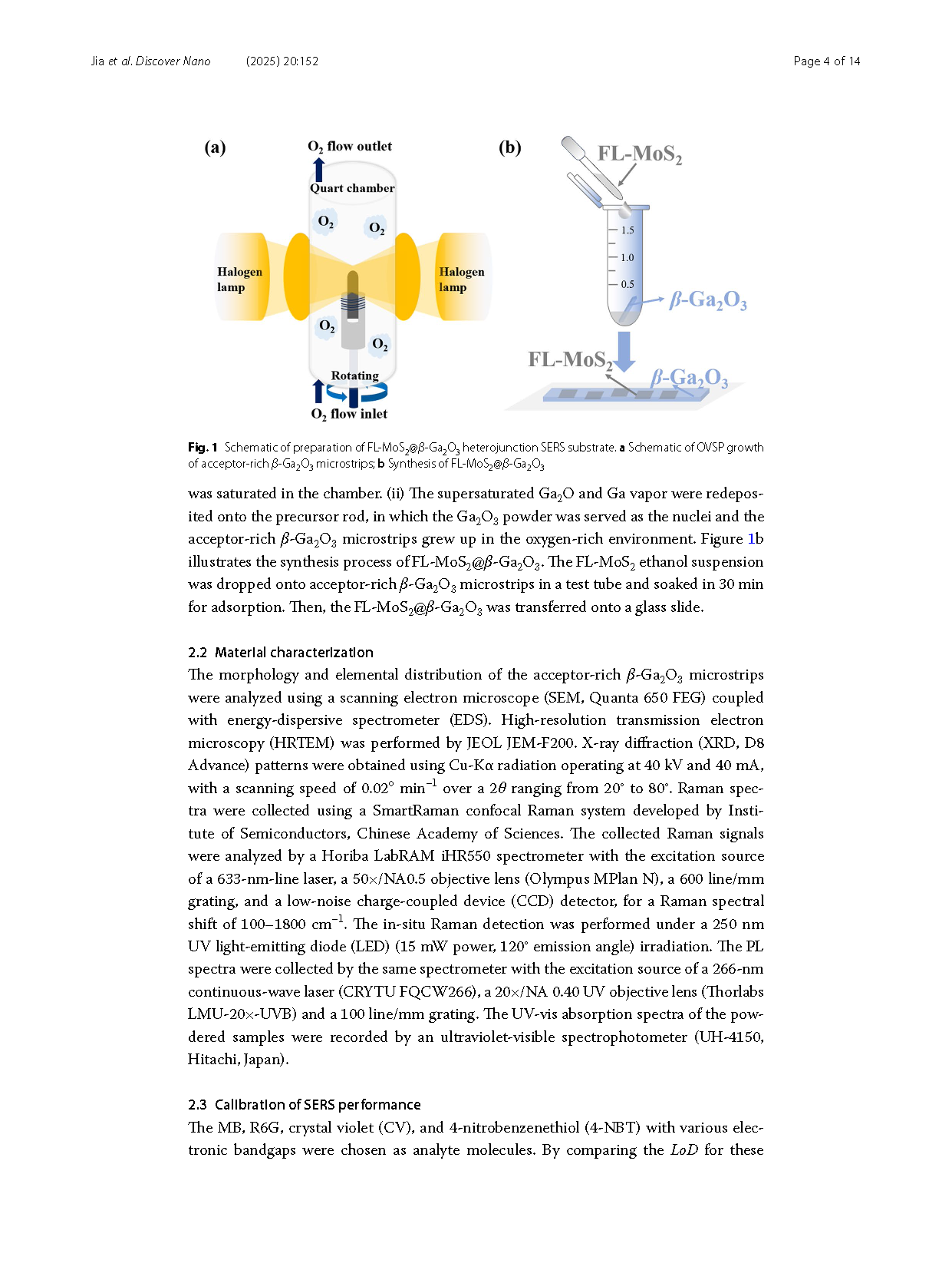
FIG.1 Schematic of preparation of FL-MoS2@β-Ga2O3 heterojunction SERS substrate. a Schematic of OVSP growth of acceptor-rich β-Ga2O3 microstrips; b Synthesis of FL-MoS2@β-Ga2O3.
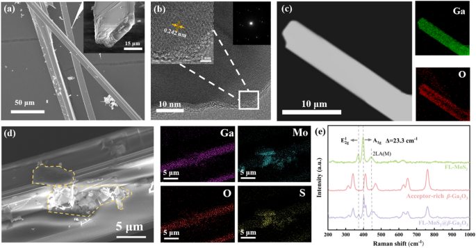
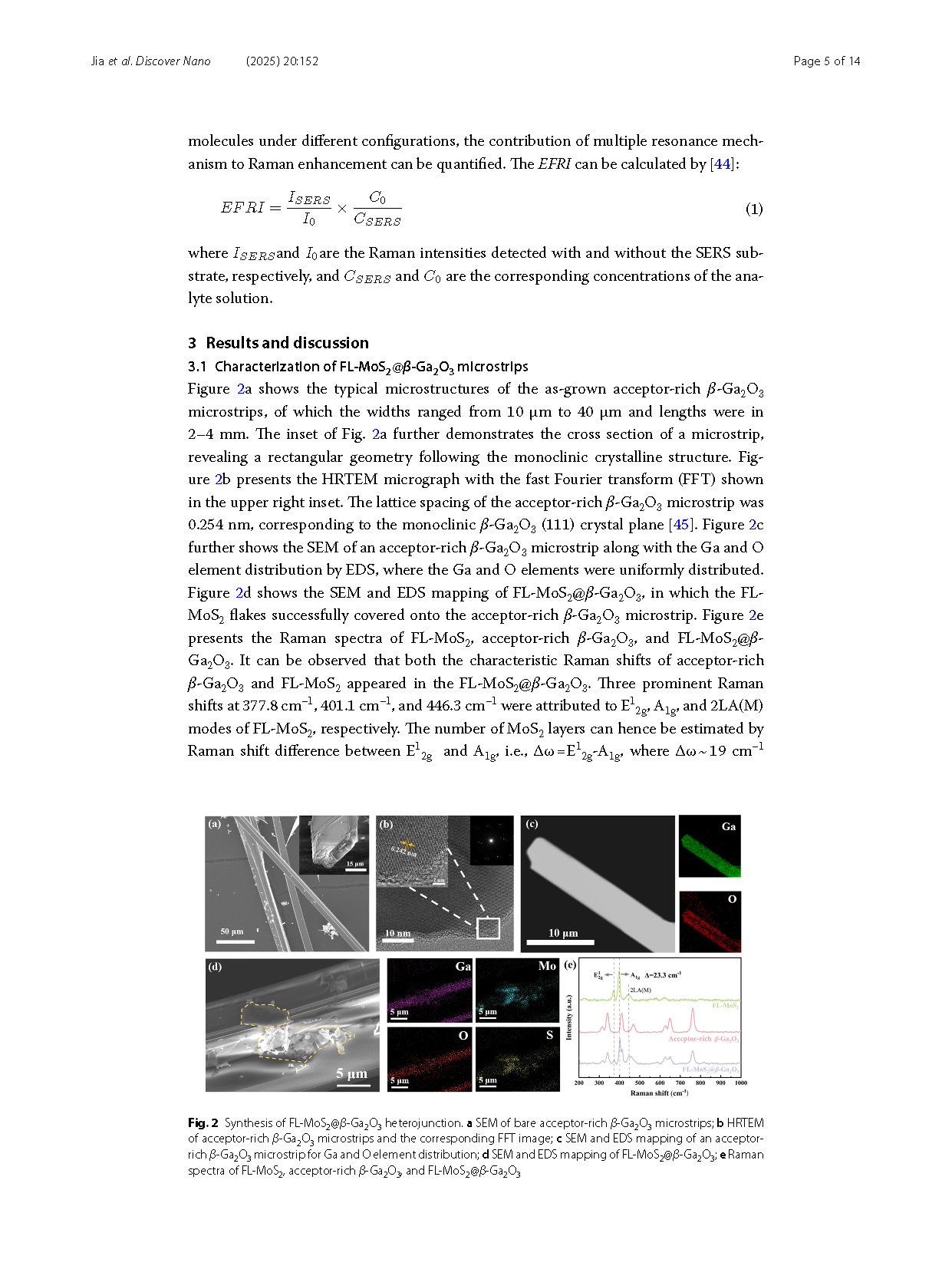
FIG.2 Synthesis of FL-MoS2@β-Ga2O3 heterojunction. (a) SEM of bare acceptor-rich β-Ga2O3 microstrips; (b) HRTEM of acceptor-rich β-Ga2O3 microstrips and the corresponding FFT image; c SEM and EDS mapping of an acceptor-rich β-Ga2O3 microstrip for Ga and O element distribution; (d) SEM and EDS mapping of FL-MoS2@β-Ga2O3; (e) Raman spectra of FL-MoS2, acceptor-rich β-Ga2O3, and FL-MoS2@β-Ga2O3.
DOI:
doi.org/10.1186/s11671-025-04339-y