Paper Sharing
【International Papers】Deep level defects in MOCVD-grown β-(AlₓGa₁₋ₓ)₂O₃
日期:2025-09-22阅读:509
Researchers from the Ohio State University have published a dissertation titled " Deep level defects in MOCVD-grown β-(AlxGa1−x)2O3" in Journal of Applied Physics.
Background
Beta-phase gallium oxide (β-Ga₂O₃) has emerged as a promising ultra-wide bandgap (UWBG) semiconductor for high-voltage and RF electronic devices due to its large bandgap (~4.8 eV), high breakdown field, and availability of large-area melt-grown substrates. Various device structures, including MESFETs and MOSFETs, have demonstrated excellent performance with high breakdown voltages and large drain currents. More recently, β-(Al₁₋ₓGaₓ)₂O₃/Ga₂O₃ heterojunction-based MODFETs have attracted attention, offering two-dimensional electron gas (2DEG) channels with high mobility and sheet charge density. However, trap states within the barrier and interface can significantly degrade device performance by increasing leakage, reducing ON/OFF ratios, and introducing noise. While prior studies have focused on structural properties and alloy behavior of β-(Al₁₋ₓGaₓ)₂O₃, little to no information exists at present regarding the presence and properties of deep level defects that act as traps in epitaxial β-(AlₓGa₁₋ₓ)₂O₃ . This work provides a systematic exploration of trap states within a range of compositions from 3% to 10% Al content and uses prior results on 0% Al (i.e., β-Ga₂O₃) as a control comparison.
Abstract
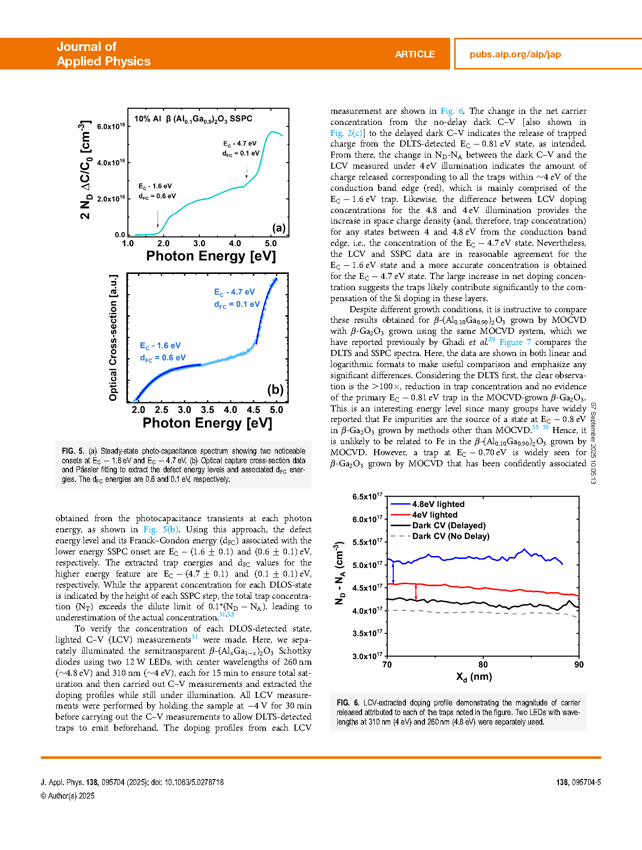
The properties of deep level defects within Si-doped β-(Al0.10Ga0.90)2O3 epitaxial layers grown by metalorganic chemical vapor deposition (MOCVD) were characterized by deep level optical spectroscopy and deep level transient (thermal) spectroscopy. Three dominant defect states are EC−0.81 eV, EC−1.6 eV, and EC−4.7 eV, while a weaker level is detected at EC−0.37 eV. Lighted C–V measurements show a consistent trend between trap concentrations increasing with the Al content and measured net doping, suggesting that these deep levels are responsible for significant carrier compensation from the Si donors. Comparisons with prior work on MOCVD-grown β-Ga2O3 layers revealed that total trap concentrations in the β-(Al0.10Ga0.90)2O3 alloy can be as much as 10–100 times larger than those of β-Ga2O3 for samples grown in the same MOCVD system. The role of Al alloying in the formation of defects was further explored by studying a separate set of β- (AlxGa1−x)2O3 samples, ranging from x = 3% to 10%. The deep level spectra exhibit consistent sets of four defect states for all β-(AlxGa1−x)2O3 samples. Comparison of deep level spectra between compositions shows a monotonic increase in trap activation energies and trap concentrations as the Al content, and bandgap, increases. Considering the variation of bandgap and conduction band offset energies, the trend among individual traps implies that these states may follow or partly follow a vacuum-referred binding energy model, useful in predicting the trap positions at higher Al-content alloys of interest for modulation-doped field effect transistors and ultraviolet photodetectors.
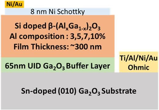
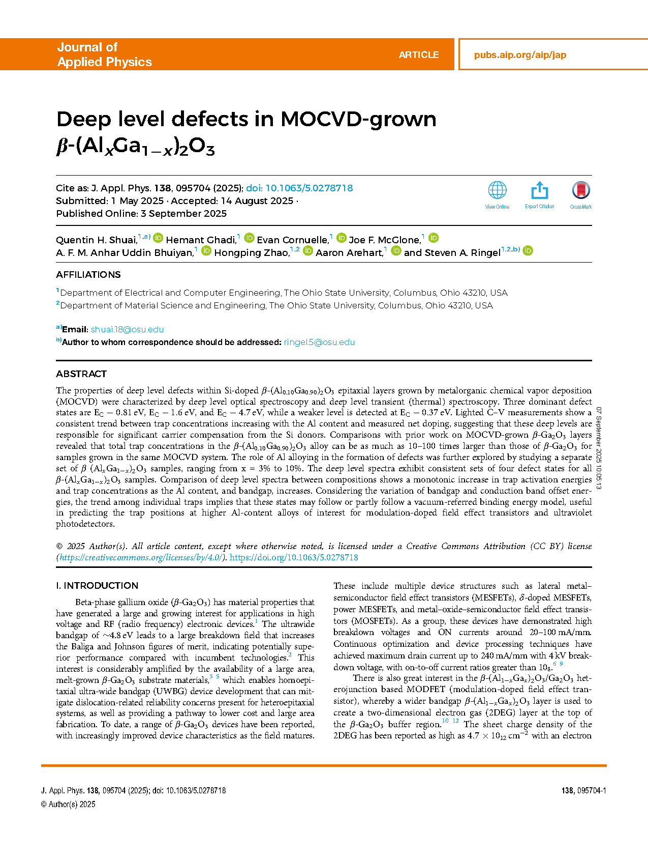
FIG. 1. Schematic rendering of the Schottky diode cross section showing the thin Ni metal to facilitate optical based measurements of the epitaxial β-(AlxGa1−x)2O3 layer, mesa isolation, and ohmic metal contacts.
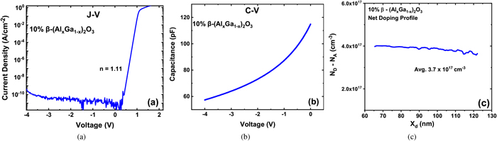
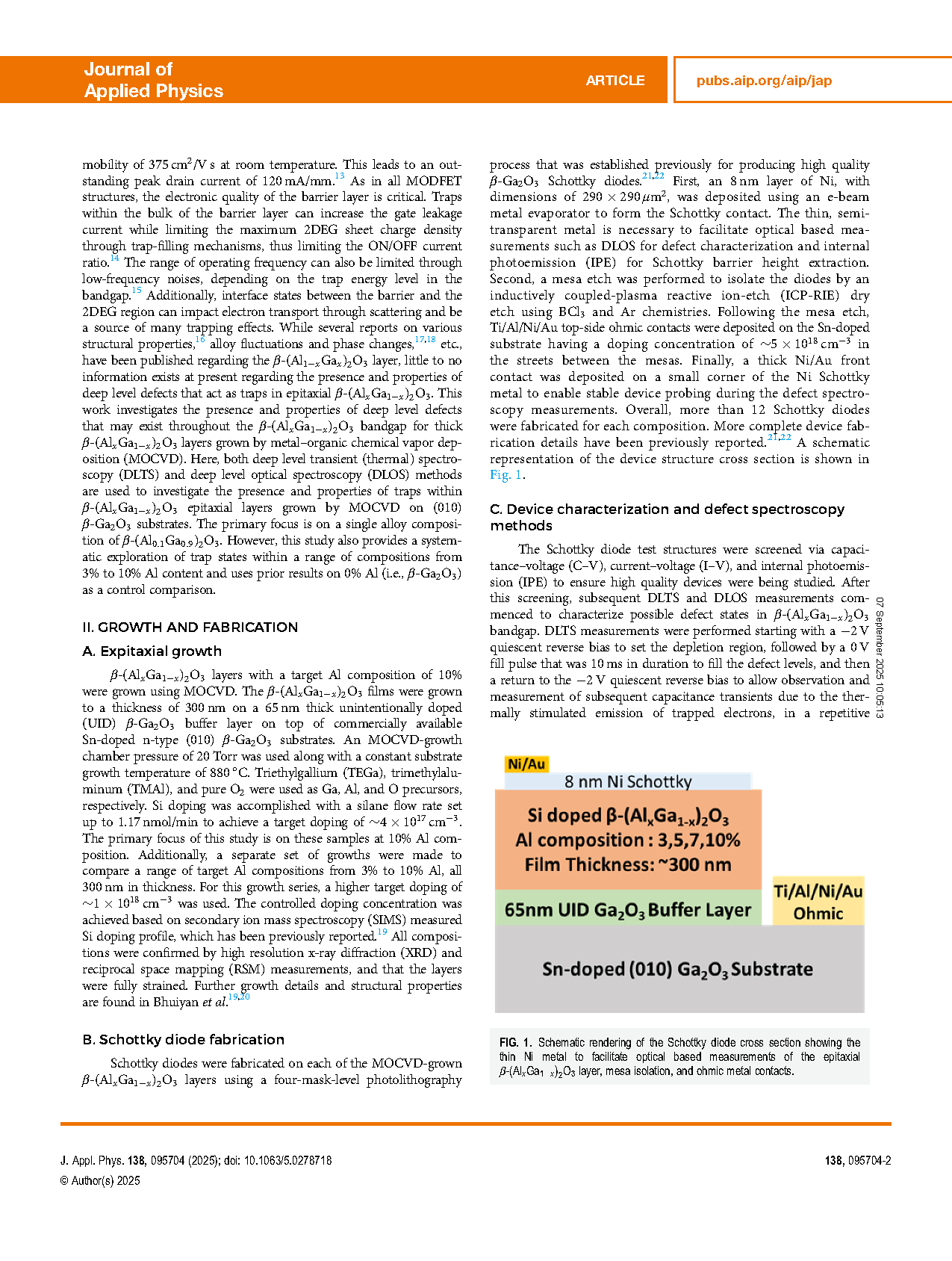
FIG. 2. Electrical measurements to characterize and qualify the Ni/β-(Al0.10Ga0.90)2O3 Schottky diodes. The figures show (a) the room temperature dark J–V, (b) C–V, and (c) extracted doping profile for a device that is typical of devices measured across the sample.
DOI:
doi.org/10.1063/5.0278718