Paper Sharing
【Domestic Papers】Study of GaN Thick Films Grown on Different Nitridated Ga₂O₃ Films
日期:2025-08-21阅读:441
Researchers from the Nanjing University have published a dissertation titled "Study of GaN Thick Films Grown on Different Nitridated Ga2O3 Films" in Crystals.
Project Support
This work is supported by Project supported by National Natural Science Foundation of China (No. 62404097), National Key R&D Program of China (2022YFB3605204, 2022YFB3605201) Fund from the Solid-State Lighting and Energy-Saving Electronics Collaborative Innovation Center and PAPD.
Background
Gallium nitride (GaN), as one of the III-nitride semiconductor materials, has been widely studied for the preparation of high-performance optoelectronic and high-power electronic devices due to its wide bandgap, high electron mobility, and excellent physical properties. GaN-based light-emitting and photodetection devices cover the entire wavelength range from ultraviolet to visible, which plays an important role in the transmitting and receiving ends of optical wireless communication systems. Recently, GaN substrates with low threading dislocation density (less than 104–105 cm−2) and low residual strain have shown potential for use in the homoepitaxial growth of GaN-based devices and show promise to further enhance GaN-based device performance. However, the high price, small size, and inconsistent quality of free-standing GaN (FS-GaN) has limited its applications.
Abstract
In this paper, various Ga2O3 films, including amorphous Ga2O3 films, β-Ga2O3, and α-Ga2O3 epitaxial films, have been nitridated and converted to single-crystalline GaN layers on the surface. Although the original Ga2O3 films are different, all the converted GaN layers exhibit the (002) preferred orientation and the porous morphologies. The ~200 µm GaN thick films have been grown on the nitridated Ga2O3 films using the halide vapor phase epitaxy (HVPE) method. Raman analysis indicates that all the HVPE-GaN films grown on nitridated Ga2O3 films are almost stress-free. An obvious GaN porous layer/Ga2O3 structure has been observed in the interface between GaN thick films and sapphire substrates. The porous GaN layers can be used as promising templates for the preparation of free-standing GaN substrates.
Conclusions
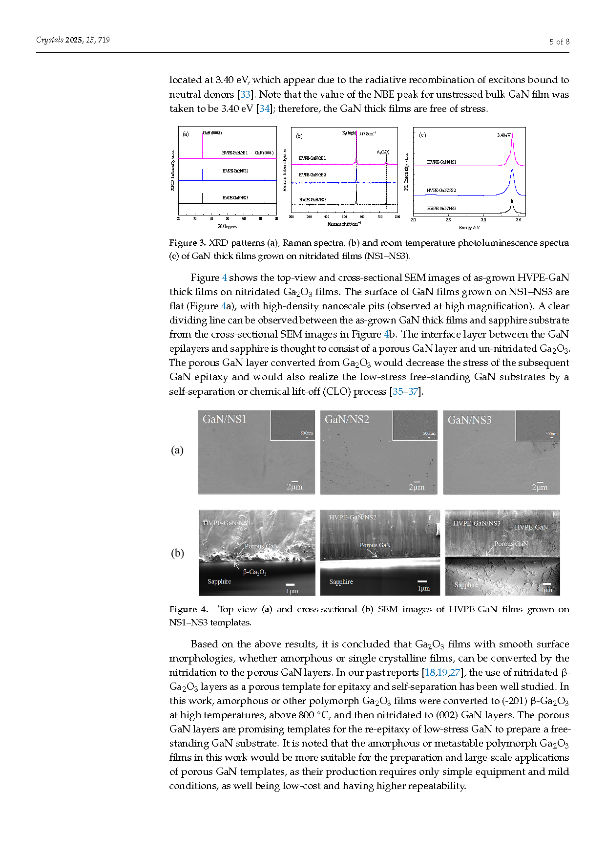
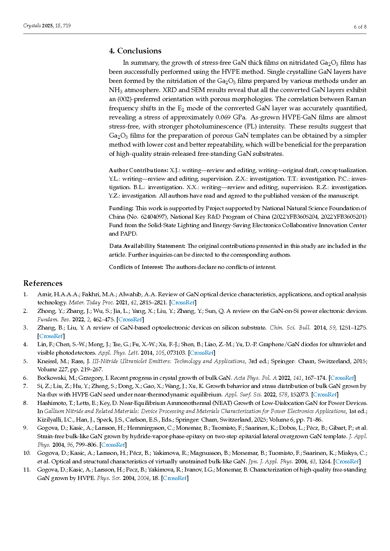
In summary, the growth of stress-free GaN thick films on nitridated Ga2O3 films has been successfully performed using the HVPE method. Single crystalline GaN layers have been formed by the nitridation of the Ga2O3 films prepared by various methods under an NH3 atmosphere. XRD and SEM results reveal that all the converted GaN layers exhibit an (002)-preferred orientation with porous morphologies. The correlation between Raman frequency shifts in the E2 mode of the converted GaN layer was accurately quantified, revealing a stress of approximately 0.069 GPa. As-grown HVPE-GaN films are almost stress-free, with stronger photoluminescence (PL) intensity. These results suggest that Ga2O3 films for the preparation of porous GaN templates can be obtained by a simpler method with lower cost and better repeatability, which will be beneficial for the preparation of high-quality strain-released free-standing GaN substrates.
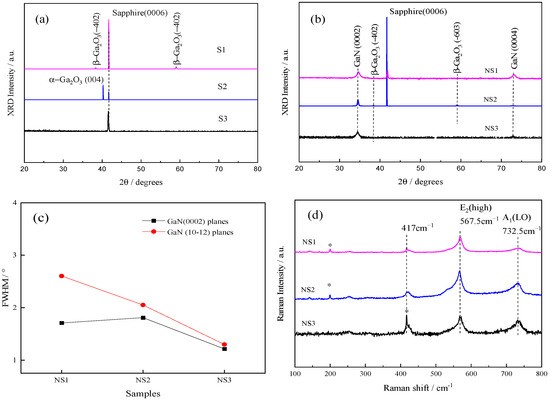
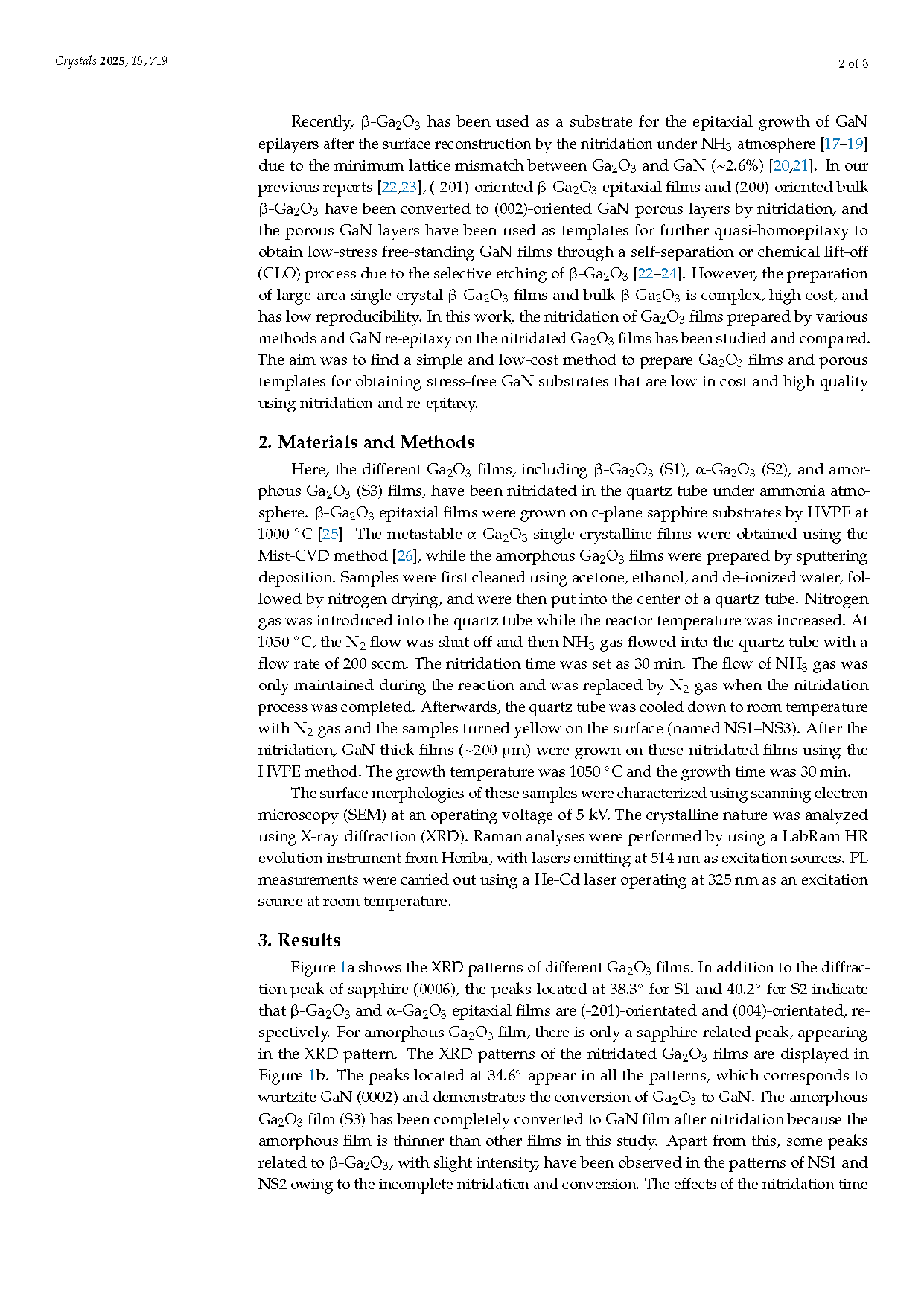
Figure 1. XRD patterns of S1–S3 samples (a) and NS1–NS3 samples (b). FWHM values of converted GaN (002) and (102) planes (c). Raman spectra of NS1–NS3 samples (d).
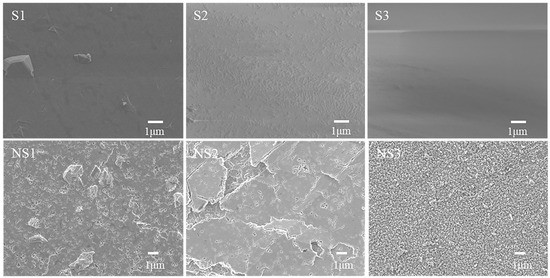
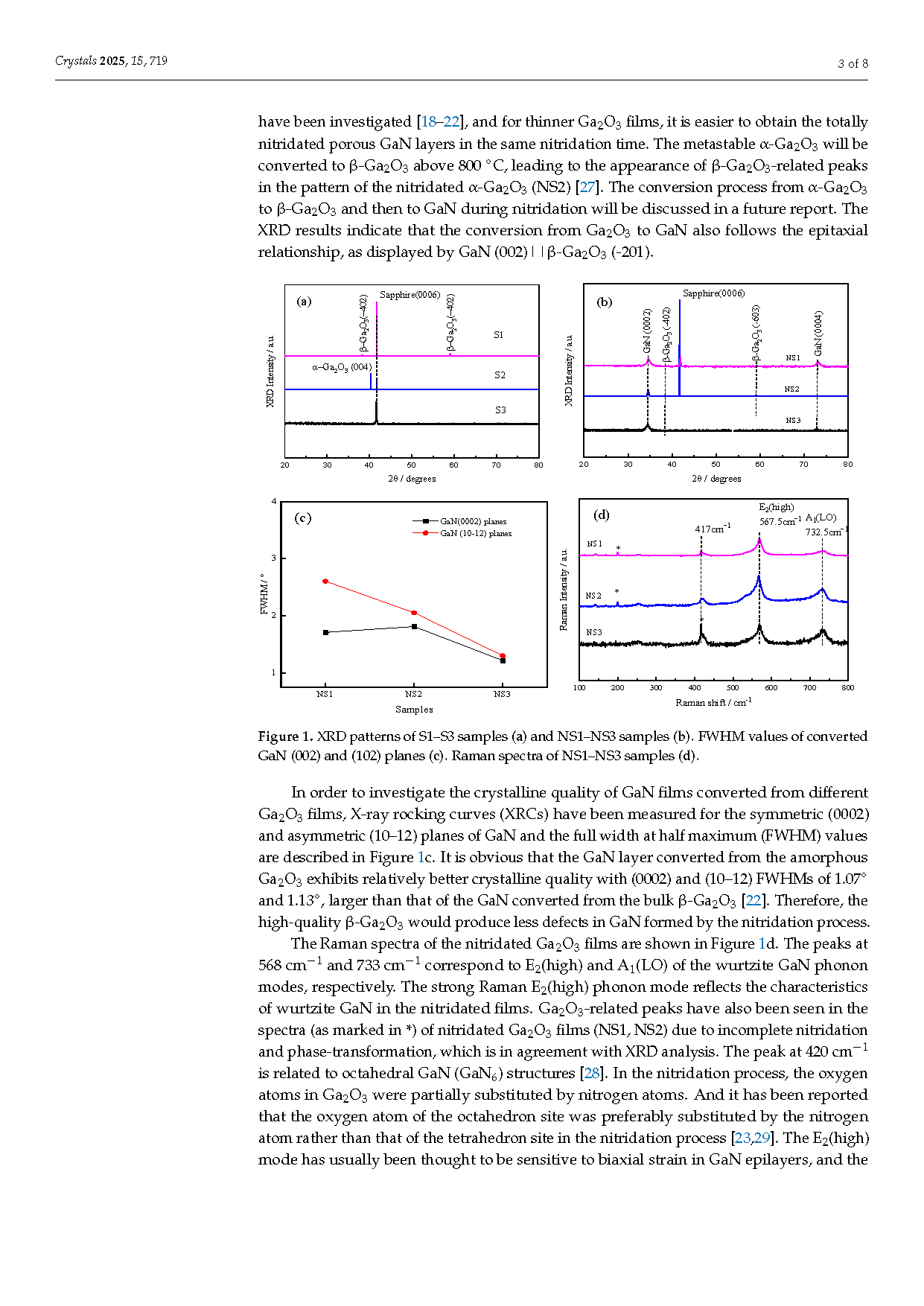
Figure 2. Top-view SEM images of S1–S3 and NS1–NS3 samples.
DOI:
doi.org/10.3390/cryst15080719