


Member News
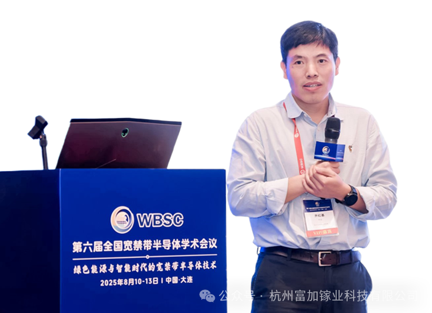
【Member News】Qi Hongji, Chairman of Fujia Gallium: AI Drives China to the Forefront of Gallium Oxide Industrialization
日期:2025-08-15阅读:785
Wide band gap and ultra-wide band gap semiconductor materials are a hot topic in the international semiconductor field and also one of the strategic high points of global high-tech competition. At this industrial trend, the 6th National Wide Band Gap Semiconductor Academic Conference was held in Dalian. This conference was jointly hosted by the wide band gap Semiconductor Professional Committee of the China Nonferrous Metals Society and the Electronic Materials Branch of the Chinese Institute of Electronics, and co-organized by Dalian University of Technology, Northeast Normal University and the China Advanced Semiconductor Industry Innovation Alliance (CASA). Qi Hongji, the chairman of Fujia Gallium, was invited to attend the conference as an industry expert and delivered a keynote report at the Sub-Forum on New Wide Band Gap Materials and Devices. Based on a series of breakthroughs made by the team in promoting the industrialization of Gallium Oxide - the innovative integration of single crystal materials and AI manufacturing, the breakthrough of MOCVD/MBE homogeneous epitaxial technology, and the verification of epitaxial material devices, Qi Hongji deeply analyzed how China can take the lead in breaking through industrial technology bottlenecks and achieve global leadership in the field of next-generation semiconductor new materials.
Qi Hongji noted in his speech that ultra-wide band gap semiconductor materials hold tremendous potential in applications such as new energy vehicles, smart grids, and rail transit. The melt growth method for gallium oxide offers significant advantages in producing large-size crystals at low cost, making it the most promising ultra-wide band gap semiconductor material for rapid commercialization. Leveraging abundant raw material resources, a vast device application market, and strong national-level project support, China is building the momentum to lead global development. However, to truly achieve international leadership, it remains essential to accelerate breakthroughs in key technologies and advance industrial implementation in order to seize the commanding heights of the global industry.
Large-scale preparation is the foundation of industrialization. After breaking through the 6-inch industrialization threshold for single crystal growth, the core of technological breakthroughs lies in integrating the breakthrough progress of artificial intelligence, combining the growth of new materials with machine learning, visual recognition, etc., just like equipping crystal growth with an "autonomous driving" system, achieving intelligent control of equipment and rapid optimization and iteration of material performance, and improving the yield rate. To support the future mass production of materials.
The "one-click crystal growth" intelligent equipment developed by Fujia Gallium has undergone batch verification. The qualification rate of crystal blanks has increased to over 90%, and the related basic patents have been granted a total of 12 international patents in the United States and Japan. At present, Fujia Gallium is actively promoting the construction of 6-inch Gallium Oxide single crystal and epitaxial wafer production lines. Once the construction is completed, it will be able to achieve a production capacity of 10,000 6-inch single crystal substrates.
If the industrialization of Gallium Oxide is compared to the construction of a highway, single crystal is the "roadbed", while high-quality epitaxy is the key "pavement layer". Fujia Gallium has made a significant breakthrough in the epitaxial process. Its Gallium Oxide epitaxial films have achieved excellent performance indicators with a thickness of over 10μm (supporting 3300V high-voltage devices) and a mobility greater than 180 cm²/V·s. Most importantly, within a 6-inch range, the homogeneity of the epitaxial film thickness has been stably better than the strict industrial introduction standard of ±2%, providing a solid guarantee for the high-speed "passage" of the device.
The technological breakthroughs in single crystal and epitaxial performance of Gallium Oxide have been strongly supported by the results of device verification. Based on the 10μm thick film with homogeneous epitaxy of conductive substrates developed by Fujia Gallium, the team has achieved SBD devices approaching the theoretical indicators of Silicon Carbide devices, and has completed the 4-inch epitaxial wafer fabrication. They are currently systematically characterizing the device performance.
The critical point for the large-scale industrial application of Gallium Oxide is just around the corner, but to achieve China's leading development, it still requires the deep integration of domestic research and development institutions and the industry. As one of the first initiating units of the Ultra-Wide Band Gap Semiconductor Innovation and Development Alliance, Fujia Gallium will continue to promote efficient collaboration among the upstream and downstream of the industrial chain and strive to realize the vision of " Bringing Quality Materials to the World" as soon as possible.
Product Introduction
Equipment:
The company has developed the world's first EFG equipment equipped with "one-click crystal growth", which can meet the growth requirements of 2-6-inch crystals. Currently, it has obtained 6 domestic authorized patents and 4 international granted patents, and can provide equipment and complete process packages.
The company has independently developed fully automated VB crystal growth systems, becoming the first in China to break through the technical bottleneck of 4-inch single crystal growth and achieve the production of large-size VB single crystals. It currently holds 6 granted domestic patents and 4 granted international patents, and can supply VB equipment along with complete process packages tailored to customer requirements.
Considering the brittleness and easy-cleavage characteristics of gallium oxide, the company has also developed 2–6 inch gallium oxide single crystal substrate grinding and polishing systems. Mature grinding, polishing, and cleaning process packages are available upon request.
Single Crystal and Epitaxial Wafer:
The company has established two enterprise standards and obtained ISO9001 quality management system certification. It supplies the market with various crystal orientation Gallium Oxide single crystal substrates ranging from 10mm to 6 inches, MOCVD-grown Gallium Oxide epitaxial wafer ranging from 10mm to 4 inches, and 10mm MBE-grown Gallium Oxide epitaxial wafer.
About Fujia Gallium
Hangzhou Fujia Gallium Technology Co., LTD., founded on December 31, 2019, is the first "hard technology" enterprise registered by Hangzhou Institute of Optics and Fine Mechanics. With the vision of "Making the World Use Good Materials", the company focuses on the industrialization work of wide bandgap semiconductor Gallium Oxide materials. The core products include Gallium Oxide single crystal substrates, MOCVD epitaxial wafers, MBE epitaxial wafers, Gallium Oxide crystal growth and processing equipment. The products mainly serve the fields of power devices, microwave and radio frequency, and optoelectronic detection. The company's series of important achievements in the development of Gallium Oxide have been featured and reported by well-known media such as People's Daily, Xinhuanet, China Securities News, and The Paper.
At present, the company has won a number of honors: In 2022, it won the Zhejiang Province Science and Technology Small and Medium-Sized Enterprise; National High-Tech Enterprise in 2023; In 2024, it will be awarded as Hangzhou Enterprise High-Tech Research and Development Center and Zhejiang Special Small and Medium-Sized Enterprise. Obtain ISO9001 quality system certification in 2025 (No. 20225Q20294R0M); It undertook one Gallium Oxide project for the National Development and Reform Commission and participated in three national and provincial projects from the Ministry of Science and Technology, Zhejiang Province, and Shanghai. In addition, it has obtained 12 international patents authorized (6 in the United States and 6 in Japan), 40 domestic patents authorized, 3 trademark certification and registration of "Fujia Gallium", and 4 software copyrights (crystal growth control software of "one-click crystal growth").
