Paper Sharing
【Domestic Papers】Enhancing the Performance of Si/Ga₂O₃ Heterojunction Solar-Blind Photodetectors for Underwater Applications
日期:2025-08-14阅读:452
Researchers from the Fuzhou University have published a dissertation titled "Enhancing the Performance of Si/Ga2O3 Heterojunction Solar-Blind Photodetectors for Underwater Applications" in Nanomaterials.
Project Support
This work is supported by the Natural Science Foundation of Fujian Province (No. 2021H0048).
Background
Solar-blind photodetectors (SBPDs) exploit their insensitivity to sunlight within the 200–280 nm spectral band, enabling critical applications in space security communications, ozone layer monitoring, missile early warning, and underwater target identification. SBPDs are uniquely indispensable for underwater detection due to their inherent immunity to solar background noise, selective sensitivity to trace DUV signatures, and compatibility with the deep ultraviolet transmission window in aquatic environments. As a result, SBPDs are increasingly recognized as a key component in the development of next-generation marine exploration systems, autonomous underwater vehicles (AUVs), and underwater photodetectors.
In addition to spectral selectivity, the materials used in the underwater detection must also exhibit strong chemical stability and corrosion resistance in aqueous solutions and typically ion-rich environments. Due to their resistance to hydrolysis and surface oxidation, materials with strong chemical inertia (such as diamond, AlGaN alloys, and β-Ga2O3) are preferred. Distinct from solid-state counterparts, underwater photodetectors necessitate fully autonomous operation without external electrodes or power inputs, mandating robust self-powered characteristics in device design.
Abstract
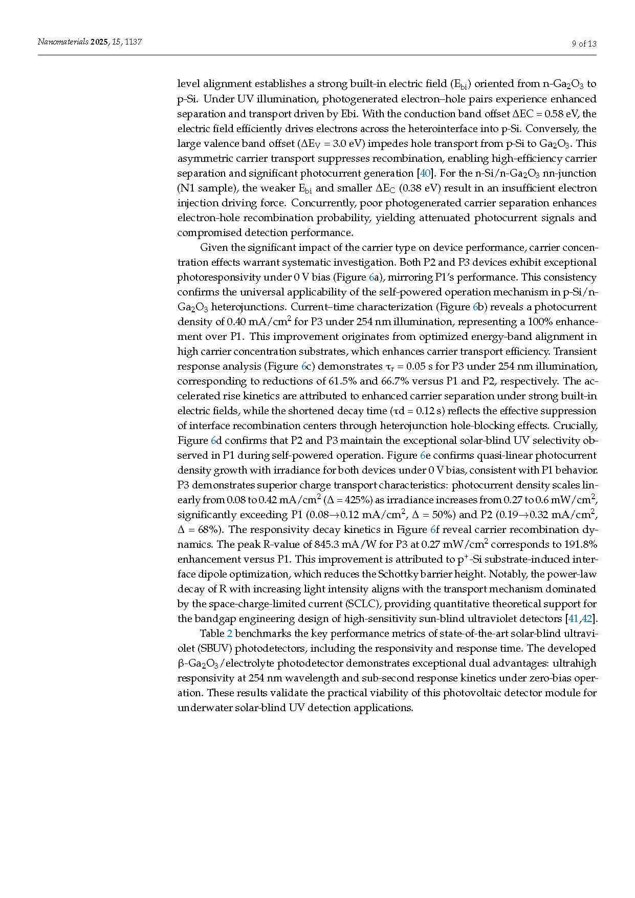
Epitaxial growth of β-Ga2O3 nanowires on silicon substrates was realized by the low-pressure chemical vapor deposition (LPCVD) method. The as-grown Si/Ga2O3 heterojunctions were employed in the Underwater DUV detection. It is found that the carrier type as well as the carrier concentration of the silicon substrate significantly affect the performance of the Si/Ga2O3 heterojunction. The p-Si/β-Ga2O3 (2.68 × 1015 cm−3) devices exhibit a responsivity of up to 205.1 mA/W, which is twice the performance of the devices on the n-type substrate (responsivity of 93.69 mA/W). Moreover, the devices’ performance is enhanced with the increase in the carrier concentration of the p-type silicon substrates; the corresponding device on the high carrier concentration substrate (6.48 × 1017 cm−3) achieves a superior responsivity of 845.3 mA/W. The performance enhancement is mainly attributed to the built-in electric field at the p-Si/n-Ga2O3 heterojunction and the reduction in the Schottky barrier under high carrier concentration. These findings would provide a strategy for optimizing carrier transport and interface engineering in solar-blind UV photodetectors, advancing the practical use of high-performance solar-blind photodetectors for underwater application.
Conclusions
In summary, well-crystallized β-Ga2O3 NRAs have been synthesized on silicon substrates by a simple one-step CVD technique. The PDs prepared on p-Si substrate with a carrier concentration of 6.48 × 1017 cm−3 exhibit an excellent responsivity of 845.3 mA/W under 254 nm illumination and 0 V bias, and the rise/decay times are 0.05 s/0.12 s. The β-Ga2O3 NARs PDs exhibit multi-periodicity and good long-term stability. The excellent performance can be attributed to the additional built-in electric field at the interface of the high carrier concentration p-type silicon substrate with the β-Ga2O3 nanowires, which promotes the effective separation of photogenerated electron–hole pairs and further prevents the fast complexation of carriers. The results demonstrate the stable operation capability of underwater photodetectors based on β-Ga2O3 NARs at 0 V bias, the high sensitivity detection performance, and the wide range of applications, revealing the great potential of this device in the field of SBUV underwater detection.
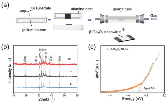
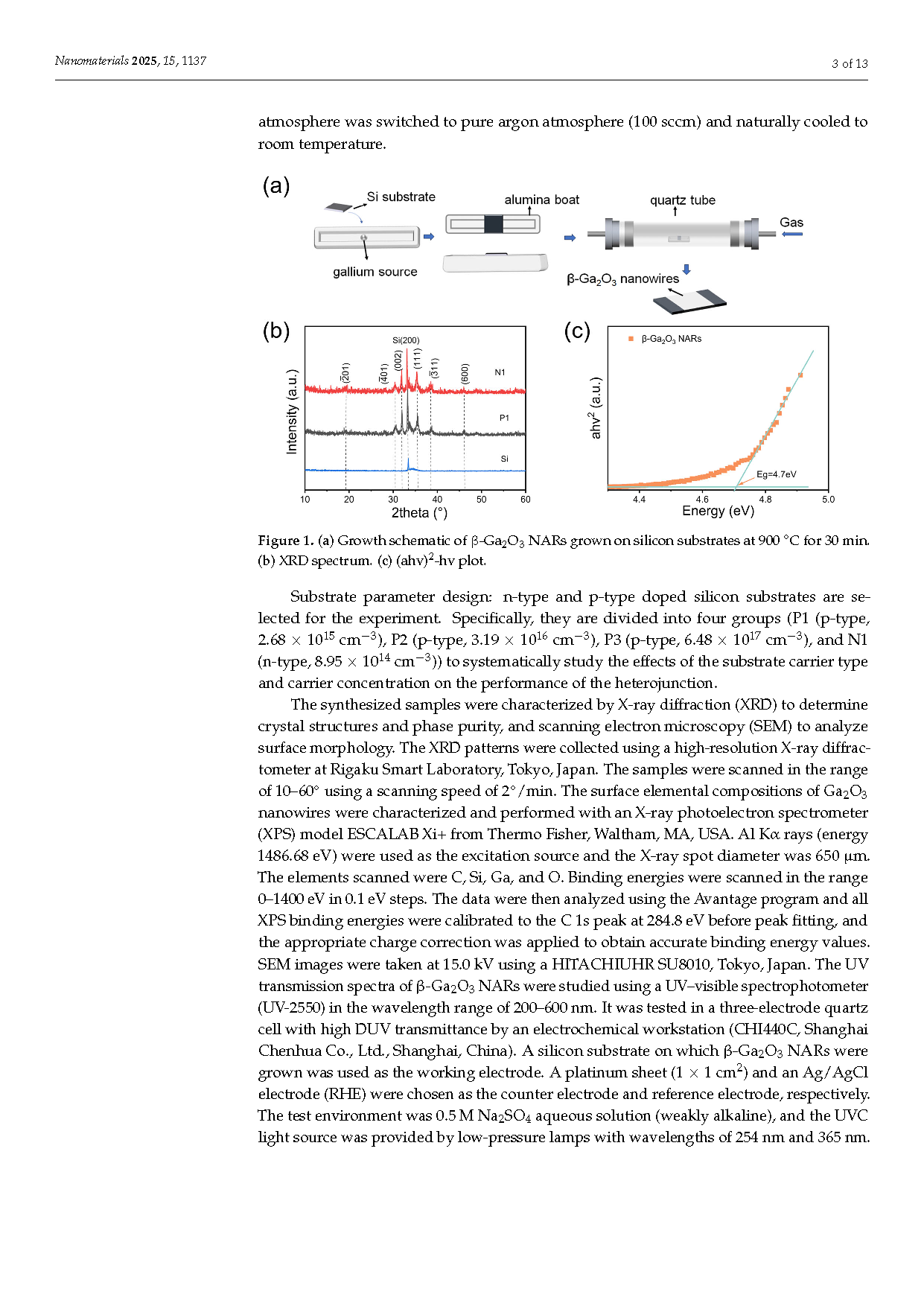
Figure 1. (a) Growth schematic of β-Ga2O3 NARs grown on silicon substrates at 900 °C for 30 min. (b) XRD spectrum. (c) (ahv)2-hv plot.
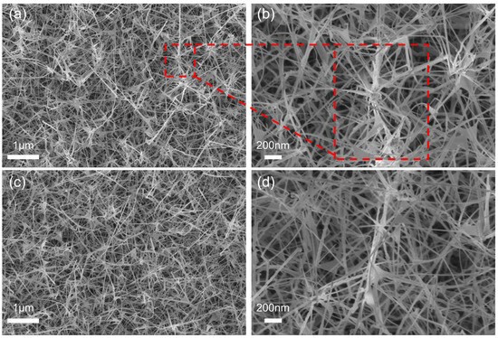
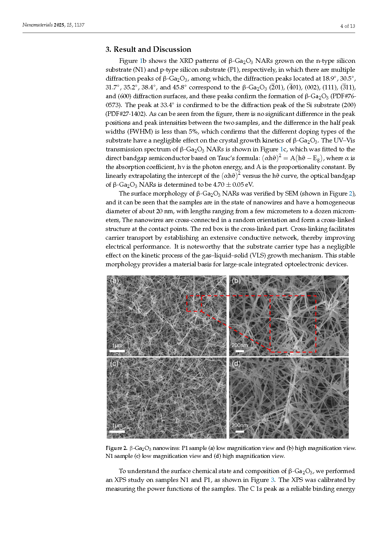
Figure 2. β-Ga2O3 nanowires: P1 sample (a) low magnification view and (b) high magnification view. N1 sample (c) low magnification view and (d) high magnification view.
DOI:
doi.org/10.3390/nano15141137