Paper Sharing
【Member Papers】Growth of Zn–N Co-Doped Ga₂O₃ Films by a New Scheme with Enhanced Optical Properties
日期:2025-07-28阅读:448
Researchers from the Xi’an Jiaotong University have published a dissertation titled "Growth of Zn–N Co-Doped Ga2O3 Films by a New Scheme with Enhanced Optical Properties" in Nanomaterials.
Project Support
This research was supported by the National Natural Science Foundation of China (grant numbers 51702253, 51332003, and M0441), the Natural Science Foundation of Shaanxi Province (No. 2022JQ-325) Key Research and Development Program of Shaanxi (2024PT-ZCK-06), and the “111 Project” of China (grant number B14040). Z.-G.Y. acknowledges support from the Natural Science and Engineering Research Council of Canada (NSERC, DG, RGPIN-2013-04416).
Background
Gallium oxide (Ga2O3) has been considered for a wide spectrum of applications in transparent conducting oxides, deep ultraviolet photodetectors, and high-voltage power electronic devices thanks to its fascinating features, such as an ultra-wide bandgap of 4.9 eV a high breakdown voltage (8 MV/cm) and a high Baliga’s figure of merit (BFOM) of around 3444. However, due to the facile presence of oxygen vacancies, Ga2O3 generally displays n-type semiconducting properties which limits its practical applications.
Doping with selective elements is an effective method to control the electronic and optical properties of semiconductors, including Ga2O3. In recent years, a series of Ga2O3-based materials with excellent properties have been successfully prepared based on this strategy The conductivity of Ga2O3 can be adjusted by doping with Sn, Ge, or Si elements and the optical bandgap of Ga2O3 semiconductors can be tuned by doping with Zn and Al. Great efforts have been made to improve the results of p-type doping of Ga2O3-based materials. Given the similar ionic radii of N3− and O2−, nitrogen is considered one of the most promising dopants for regulating the electronic and optical properties of Ga2O3-based materials. However, effective high-concentration nitrogen doping is usually difficult to achieve in most studies. Notably, high-quality nitrogen-doped p-type Ga2O3 materials were successfully prepared by the thermal oxidation of gallium nitride (GaN) on sapphire substrates at 1000–1100 °C. First-principles calculations showed that tunable optical properties and even p-type conductivity can be achieved through co-doping with Zn and N. However, it is very difficult to achieve co-doping in the experiment. So far, the influence of Zn and N co-doping on the physical properties of Ga2O3 films is still unknown experimentally. Therefore, it is rewarding to take on this challenge in this work.
Abstract
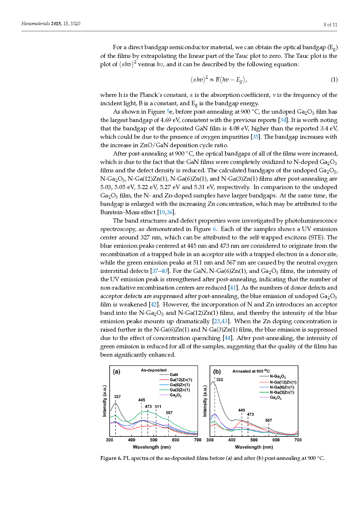
Gallium oxide (Ga2O3), as a wide-bandgap semiconductor material, is highly expected to find extensive applications in optoelectronic devices, high-power electronics, gas sensors, etc. However, the photoelectric properties of Ga2O3 still need to be improved before its devices become commercially viable. As is well known, doping is an effective method to modulate the various properties of semiconductor materials. In this study, Zn–N co-doped Ga2O3 films with various doping concentrations were grown in situ on sapphire substrates by atomic layer deposition (ALD) at 250 °C, followed by post-annealing at 900 °C. The post-annealed undoped Ga2O3 film showed a highly preferential orientation, whereas with the increase in Zn doping concentration, the preferential orientation of Ga2O3 films was deteriorated, turning it into an amorphous state. The surface roughness of the Ga2O3 thin films is largely affected by doping. As a result of post-annealing, the bandgaps of the Ga2O3 films can be modulated from 4.69 eV to 5.41 eV by controlling the Zn–N co-doping concentrations. When deposited under optimum conditions, high-quality Zn–N co-doped Ga2O3 films showed higher transmittance, a larger bandgap, and fewer defects compared with undoped ones.
Conclusions
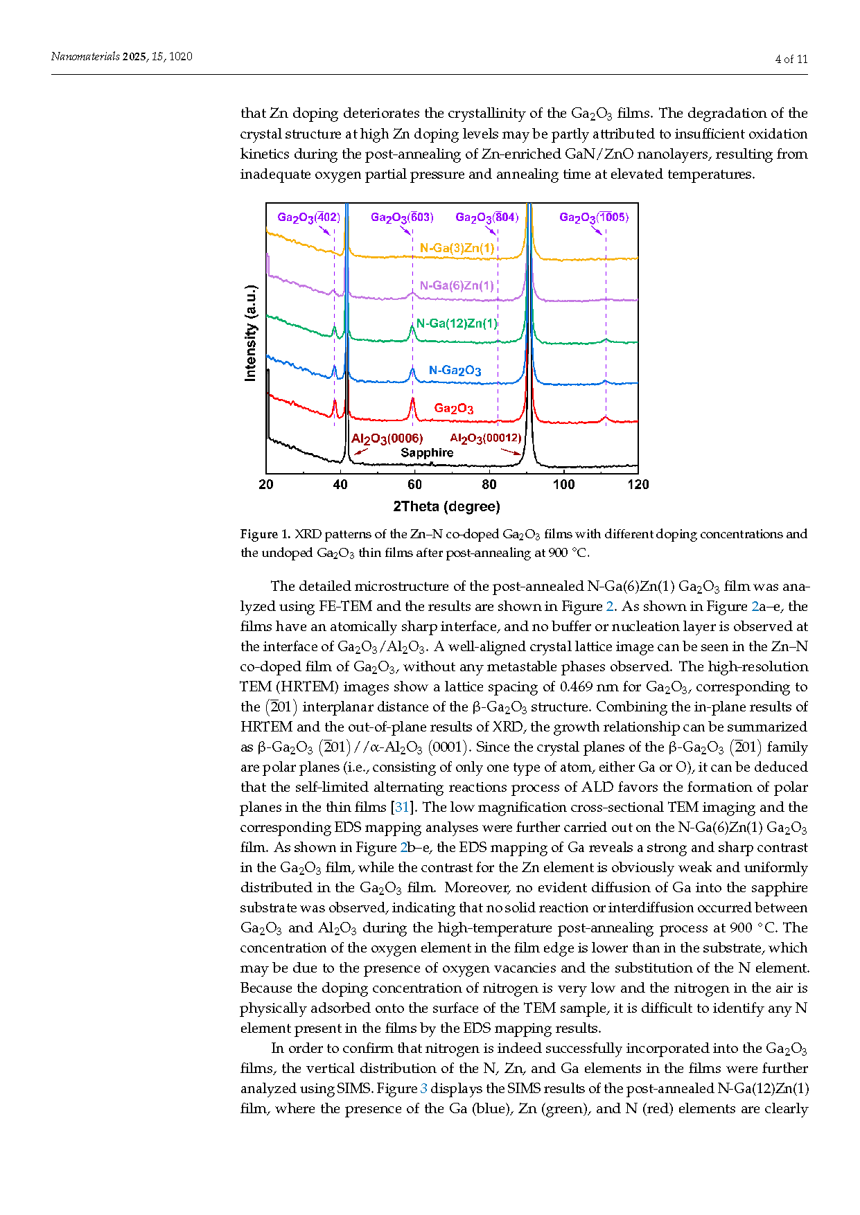
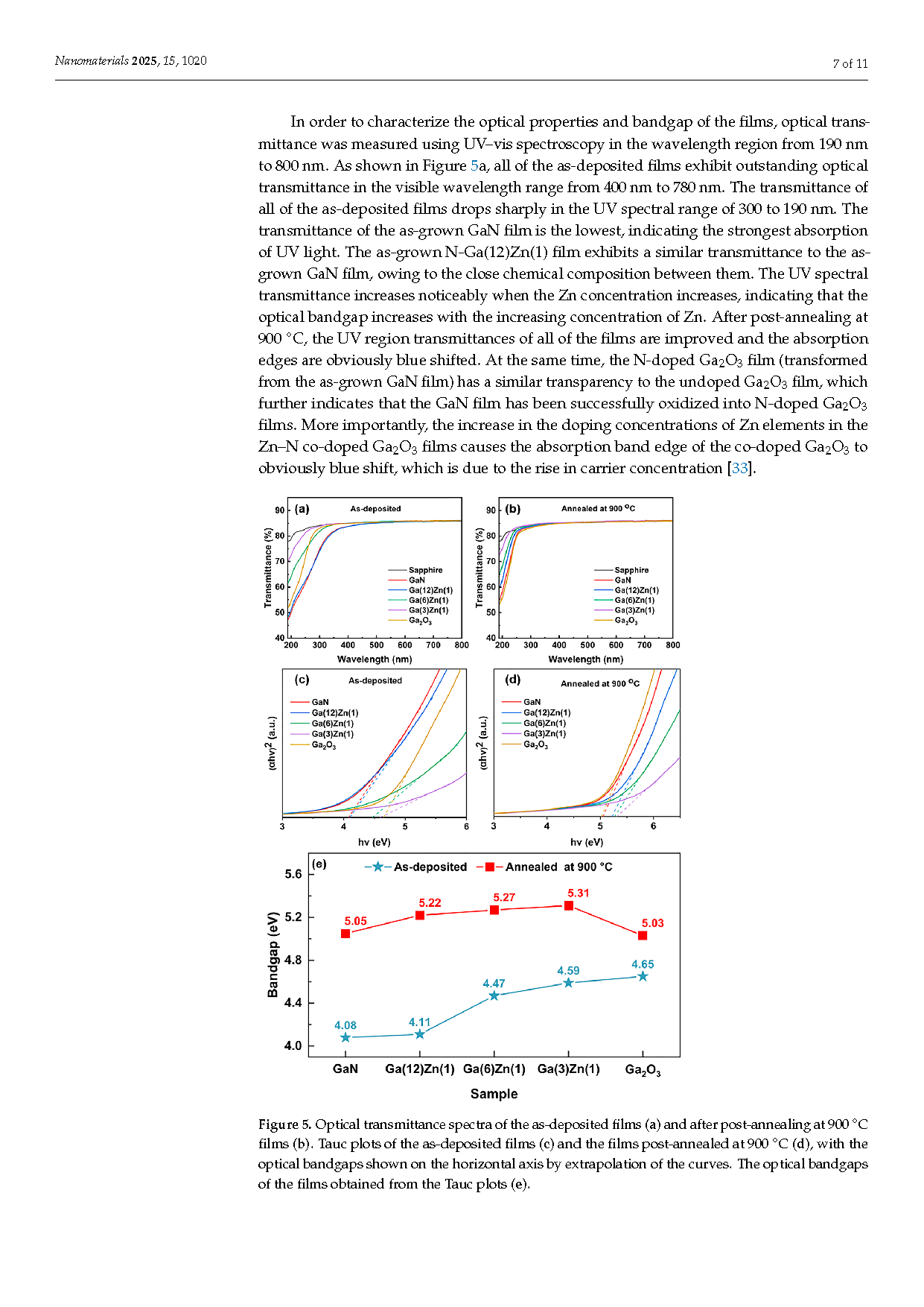
In conclusion, Zn–N co-doped Ga2O3 films have been successfully grown on sapphire substrates using ALD followed with a post-annealing process. After being post-annealed at 900 °C, all of the films transform into a highly preferentially oriented β-Ga2O3, except for the sample of N-Ga(3)Zn(1), which remains amorphous. The HRTEM results reveal that an atomically sharp interface is formed and partial epitaxial growth takes place at the N-Ga(6)Zn(1) β-Ga2O3/α-Al2O3 interface. As the Zn doping concentration increases, the surface roughness of the films was reduced from 4.27 nm to 0.154 nm. In the visible wavelength region, all of the films exhibit an ultra-high optical transmittance, and the optical transmittance increases with the Zn doping concentration in the UV wavelength region. The bandgap of the Ga2O3 films can be adjusted from 5.07 eV to 5.41 eV by changing the Zn doping concentration. The PL spectra of the films exhibit several emission centers around 327 nm, 445 nm, 473 nm, 511 nm, and 567 nm under the excitation wavelength of 280 nm. A decline in the green luminescence was observed after post-annealing, demonstrating a decrease in oxygen interstitial defects. This work demonstrates that the structural and optical properties of β-Ga2O3 film can be well tuned by Zn–N co-doping and post-annealing. These findings facilitate the development of Ga2O3-based solar-blind ultraviolet photodetectors and other optoelectronic devices.
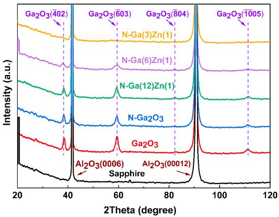
Figure 1. XRD patterns of the Zn–N co-doped Ga2O3 films with different doping concentrations and the undoped Ga2O3 thin films after post-annealing at 900 °C.
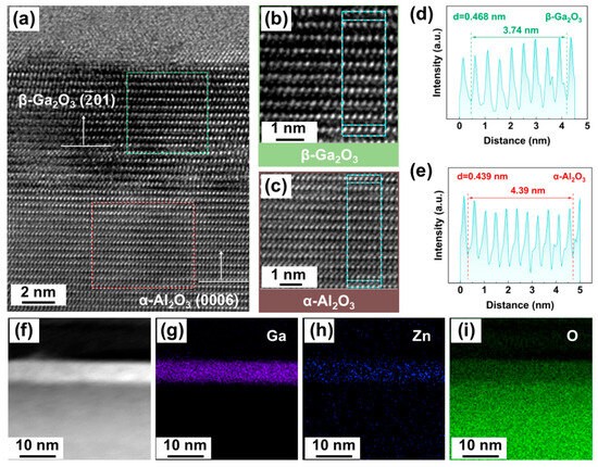
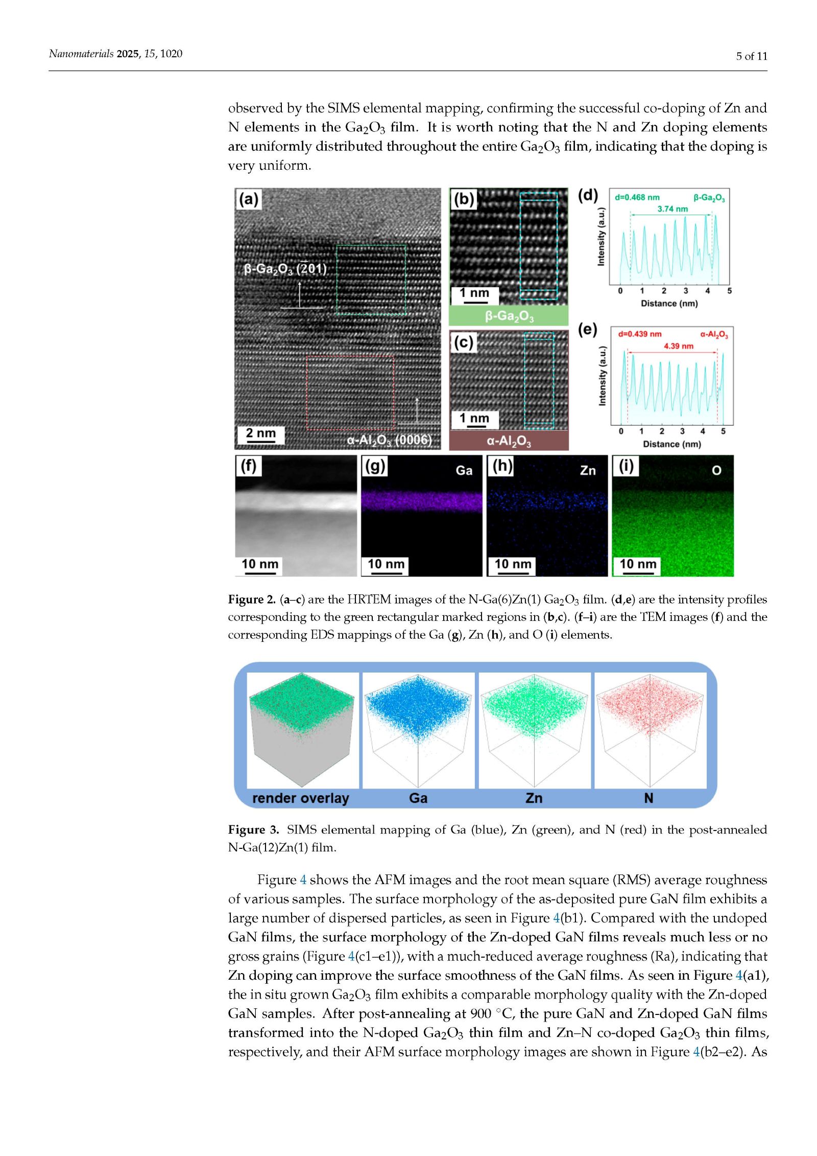
Figure 2. (a–c) are the HRTEM images of the N-Ga(6)Zn(1) Ga2O3 film. (d,e) are the intensity profiles corresponding to the green rectangular marked regions in (b,c). (f–i) are the TEM images (f) and the corresponding EDS mappings of the Ga (g), Zn (h), and O (i) elements.
DOI:
doi.org/10.3390/nano15131020