Paper Sharing
【International Papers】Structural and electrical properties of (100) β-(ScₓGa₁₋ₓ)₂O₃/Ga₂O₃ heterojunctions
日期:2025-07-28阅读:441
Researchers from the Institute of Science Tokyo have published a dissertation titled "Structural and electrical properties of (100) β-(ScxGa1−x)2O3/Ga2O3 heterojunctions" in Journal of Applied Physics.
Background
Ultrawide bandgap semiconductors have been a recent subject of intense investigation for the development of electric devices operable under harsh conditions, such as high voltages, high powers, high temperatures, and high radiations. Among candidates, monoclinic β-Ga2O3, the most stable polytype of Ga2O3, is promising owing to the availability of melt-grown large bulk single crystals with tunable electrical properties from semi-insulating to highly conductive and its sufficiently large bandgap energy (Eg) of 4.4–5.0 eV. Despite its distinctive crystal structure, bandgap engineering is viable in β-Ga2O3 through cation substitution, akin to other group III compound semiconductors such as wurtzite-type InN–GaN–AlN or corundum-type Al2O3–Ga2O3 systems. This approach enables the growth of a pseudomorphic heterostructure applicable to electronic devices. In particular, modulation-doped heterostructures, where a donor impurity is selectively doped into the barrier layer, are attractive since they form a two-dimensional electron gas (2DEG) at the interface. High-density 2DEG in β-Ga2O3 is predicted to exceed the bulk electron mobility owing to the screening of phonon scattering. Therefore, they can be applied in heterojunction field-effect transistors (HFETs) capable of high-frequency or high-voltage operation.
Abstract
Continuous composition-spread and heavily Si-doped β-(ScxGa1−x)2O3 (0.04 ≤ x ≤ 0.20) films were epitaxially grown on (100) β-Ga2O3 substrates by pulsed-laser deposition. The x dependence of structural and electrical properties was examined at room temperature. Vertical Schottky barrier diodes (SBDs) of Pt/β-(ScxGa1−x)2O3 with x ≤ 0.10 showed ideality factors of 1.6–1.7 and series resistance less than 10 mΩ cm2. In addition, the effective Schottky barrier height increased by ∼0.2 eV with increasing x from 0 to 0.10. The parasitic series resistance in SBDs with x > 0.10 increased exponentially as x increased, which was attributed to carrier localization in β-(ScxGa1−x)2O3 epilayers. This behavior was correlated with a sharp increase in the density of incoherent twin boundaries inherent in (100)-oriented β-Ga2O3-based epilayers. Moreover, the β-(ScxGa1−x)2O3/Ga2O3 interface with 0.04 ≤ x ≤ 0.11 accommodated two-dimensional electrons with a sheet density of 5–6 × 1012 cm−2, which is comparable to that observed at the (010) β-(AlxGa1−x)2O3/Ga2O3 interface. Our study demonstrates extended material designs for realizing modulation doping in β-Ga2O3 and its application to heterojunction field-effect transistors.
Conclusion
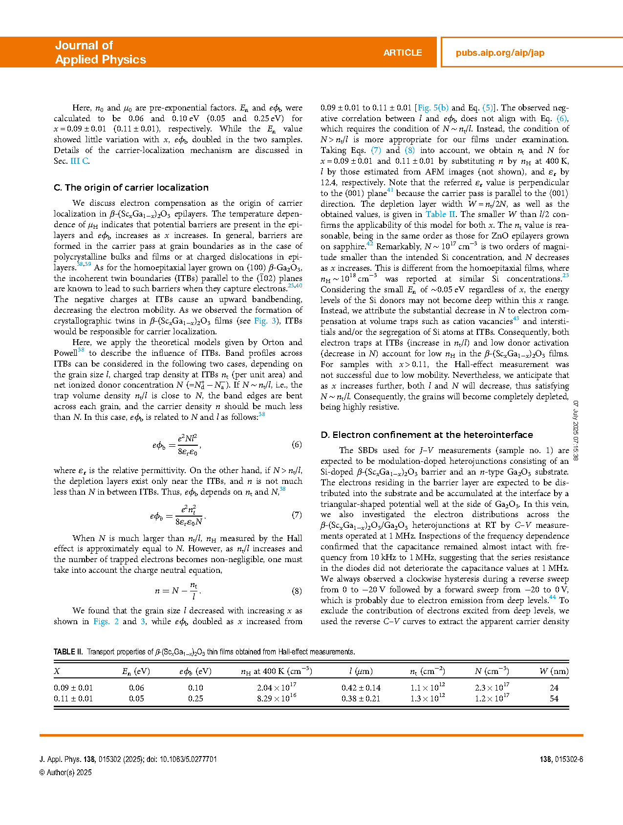
We investigated various properties of (100)-oriented β-(ScxGa1−x)2O3 epilayers as a function of x, including the electrical characteristics of SBDs with Pt electrodes and 2DEG at the interface with Ga2O3 substrates. In J–V curves for the SBDs, clear rectification behaviors were confirmed for samples with x ≤ 0.12, while an exponential increase in resistivity above x = 0.10 was ascribed to the insulation behavior of β-(ScxGa1−x)2O3 epilayers. In addition, we found that the linear increase in ϕSBH,eff corresponds to ΔEg(x). From AFM and EBSD inspections, the surface morphology and microscopic crystal orientation were found to influence the temperature-dependent transport properties as well as the insulation behavior. In short, all these results could be explained in terms of the characteristic size of grains in between ITBs inherent in (100)-oriented β-Ga2O3-based epilayers and ionized donor concentration, both of which decreased as x increased. The carrier density profiles at the (100) β-(ScxGa1−x)2O3/Ga2O3 interface revealed the formation of a 2DEG with a sheet density of 5–6 × 1012 cm−2 for x ≤ 0.11. This value is comparable to that obtained for (010) β-(AlxGa1−x)2O3/Ga2O3. Although the doping efficiency of Si donors in the present samples is limited, particularly above x = 0.10, our results contribute to the continuous development of high-performance heterojunction devices based on β-Ga2O3.
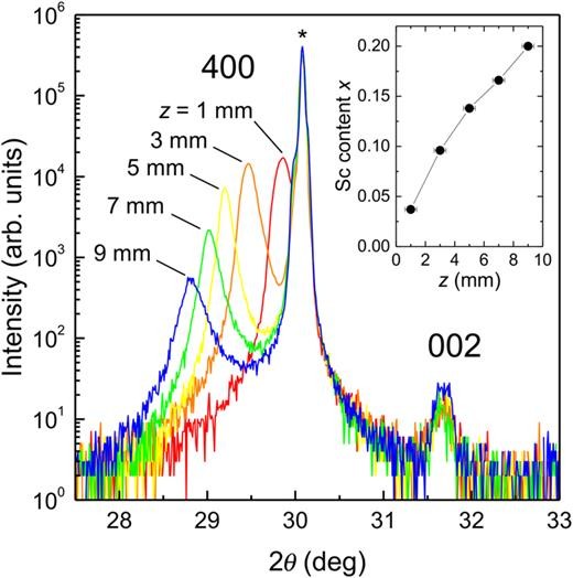
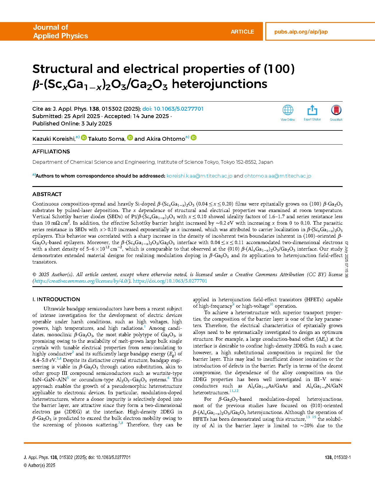
FIG.1 Out-of-plane XRD profiles around 400 reflections for sample no. 1. The reflection labeled by an asterisk (*) comes from (100) β-Ga2O3 substrates. The inset shows the variation in Sc content x along the lateral length z with error bars corresponding to a spot size of the incident x ray.
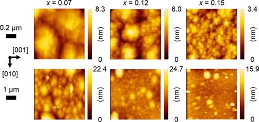
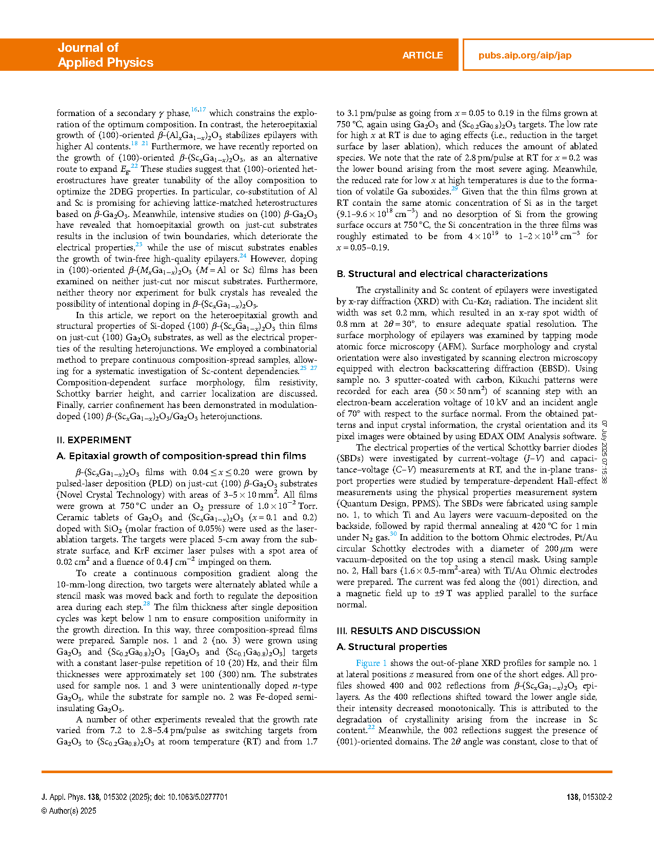
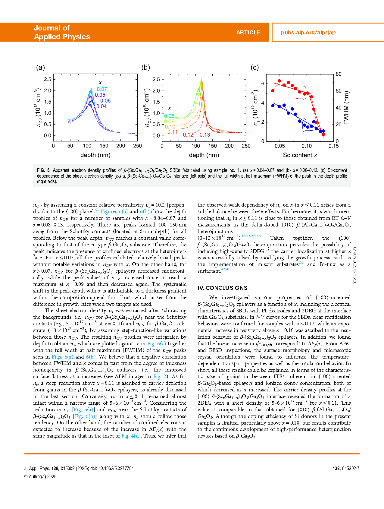
FIG.2 AFM images of sample no. 1 in the regions with x = 0.07, 0.12, and 0.15. The scanned areas are 1 × 1 and 5 × 5 μm2 for top and bottom panels, respectively. Black arrows represent crystal orientations.
DOI:
doi.org/10.1063/5.0277701