Paper Sharing
【Domestic Papers】Modulation of defect structures for MOCVD-grown ε-Ga₂O₃ thin films by using sapphire substrates with large off-axis angles
日期:2025-07-25阅读:500
Researchers from the Sun Yat-sen University have published a dissertation titled "Modulation of defect structures for MOCVD-grown ε-Ga2O3 thin films by using sapphire substrates with large off-axis angles" in Applied Surface Science.
Project Support
This work was supported by the Natural Science Foundation of China (Grant No. 62074167), the Research and Development Plan Project of Guangdong Province (No. 2021B0101300005).
Background
The meta-stable ε-Ga2O3 is an attractive wide-bandgap semiconductor material, characterized by its ultrawide bandgap (4.9 eV), high breakdown electric field strength (8 MV/cm), and large spontaneous polarization (23 μC/cm2). It holds potential for applications in solar-blind ultraviolet (UV) detectors, high electron mobility transistors (HEMTs), Schottky barrier diodes (SBDs) and metal–oxide–semiconductor field-effect transistors (MOSFETs). However, the high density of defects in heteroepitaxial ε-Ga2O3 degrades device performance. Additionally, achieving a theoretically high density of two-dimensional electron gas (2DEG) at the ε-Ga2O3-based heterointerface is challenging in experiments due to the lack of high crystalline quality ε-Ga2O3 and suitable device-level surfaces for growing heterostructures. Therefore, commercial applications for ε-Ga2O3-based devices still face significant challenges.
Abstract
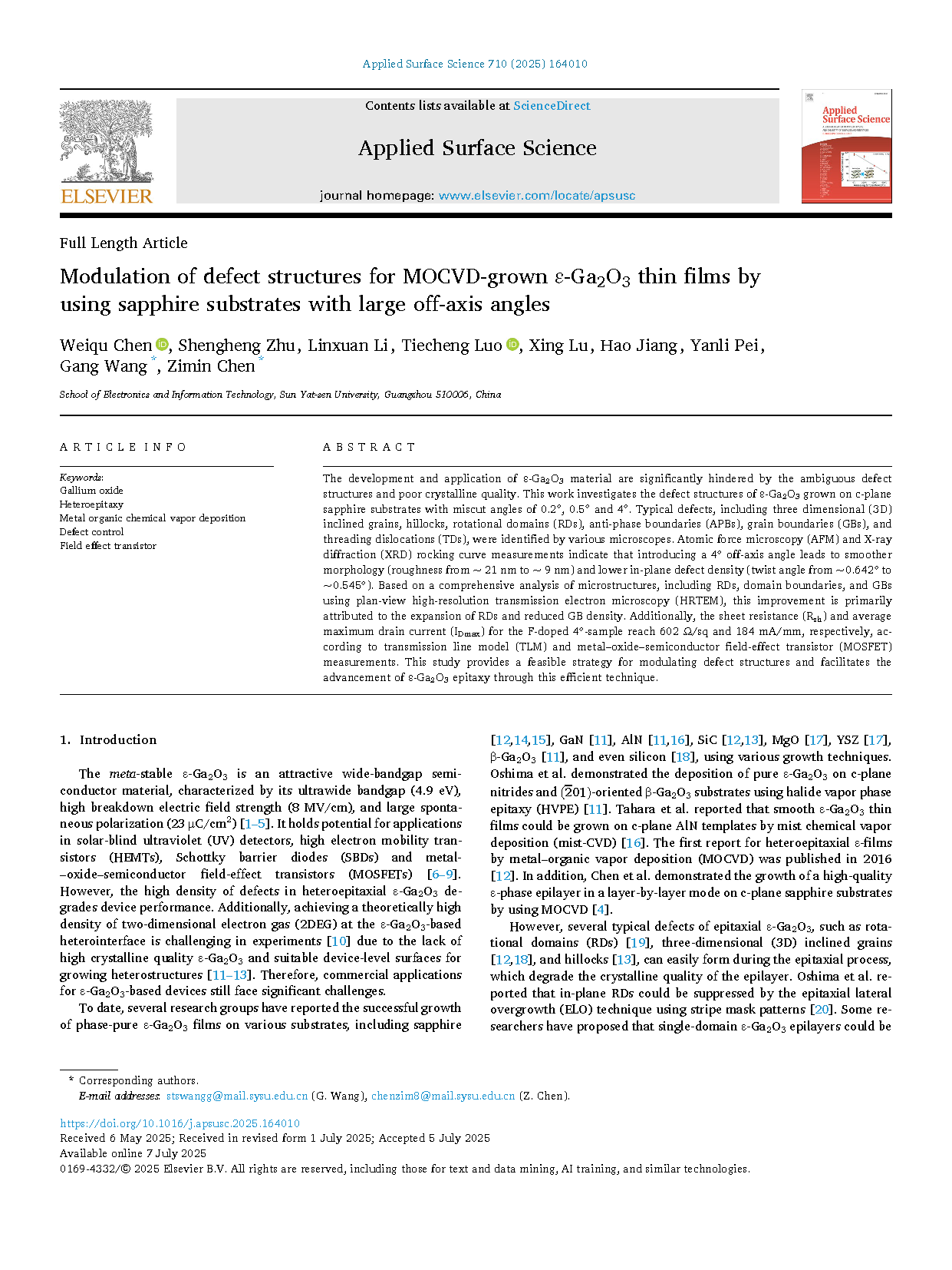
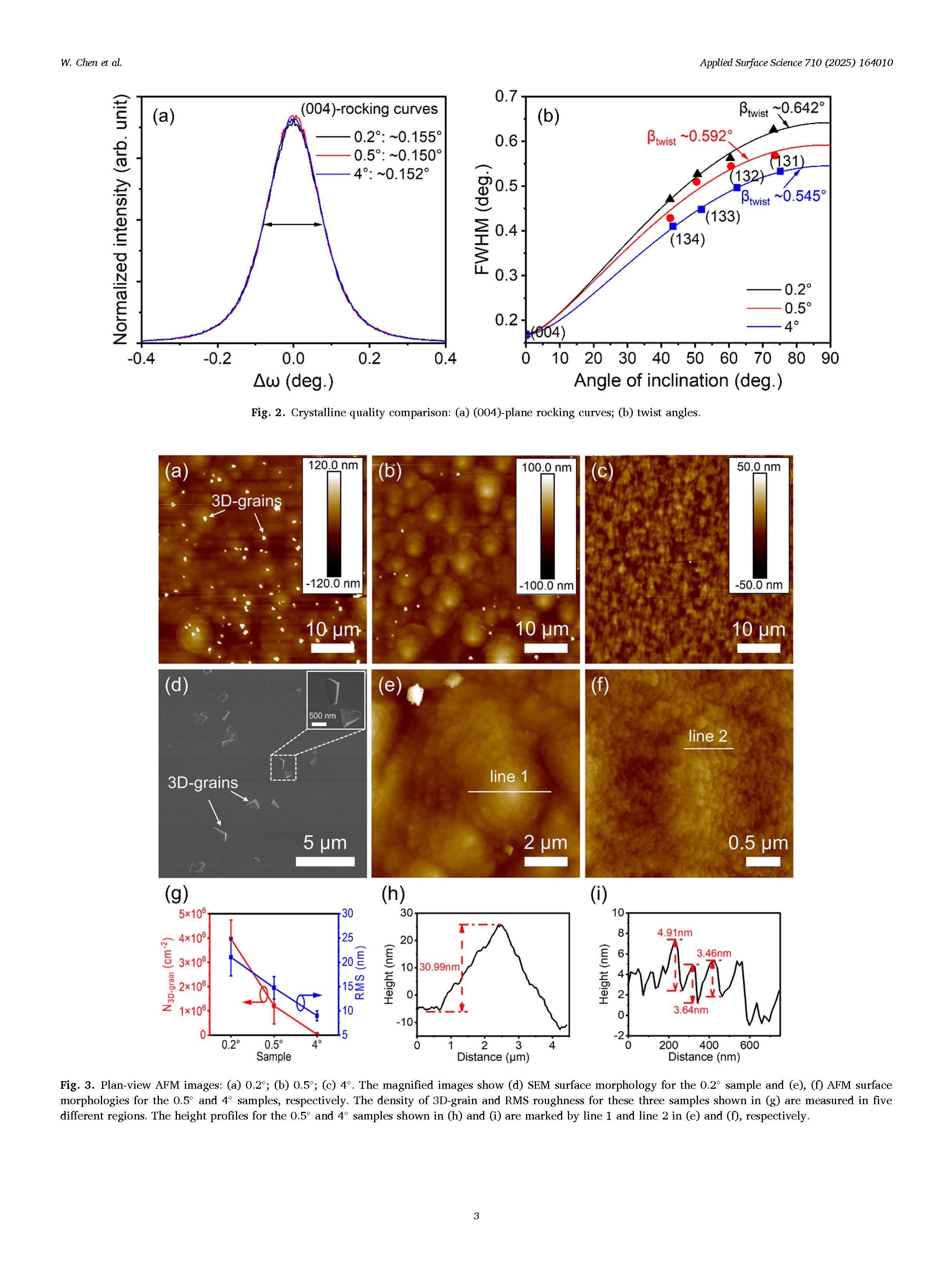
The development and application of ε-Ga2O3 material are significantly hindered by the ambiguous defect structures and poor crystalline quality. This work investigates the defect structures of ε-Ga2O3 grown on c-plane sapphire substrates with miscut angles of 0.2°, 0.5° and 4°. Typical defects, including three dimensional (3D) inclined grains, hillocks, rotational domains (RDs), anti-phase boundaries (APBs), grain boundaries (GBs), and threading dislocations (TDs), were identified by various microscopes. Atomic force microscopy (AFM) and X-ray diffraction (XRD) rocking curve measurements indicate that introducing a 4° off-axis angle leads to smoother morphology (roughness from ∼ 21 nm to ∼ 9 nm) and lower in-plane defect density (twist angle from ∼0.642° to ∼0.545°). Based on a comprehensive analysis of microstructures, including RDs, domain boundaries, and GBs using plan-view high-resolution transmission electron microscopy (HRTEM), this improvement is primarily attributed to the expansion of RDs and reduced GB density. Additionally, the sheet resistance (Rsh) and average maximum drain current (IDmax) for the F-doped 4°-sample reach 602 Ω/sq and 184 mA/mm, respectively, according to transmission line model (TLM) and metal–oxide–semiconductor field-effect transistor (MOSFET) measurements. This study provides a feasible strategy for modulating defect structures and facilitates the advancement of ε-Ga2O3 epitaxy through this efficient technique.
Highlights
● Typical defects in ε-Ga2O3include surface defects and in-plane defects.
● Quasi step-flow ε-Ga2O3films on large off-axis sapphire substrates were achieved.
● In-plane defect density of ε-Ga2O3decreased using off-axis sapphire substrates.
● The ε-Ga2O3grains consist of several rotational domains and anti-phase boundaries.
● The sheet resistance for the fluorine-doped 4°-sample is 602 Ω/sq.
Conclusion
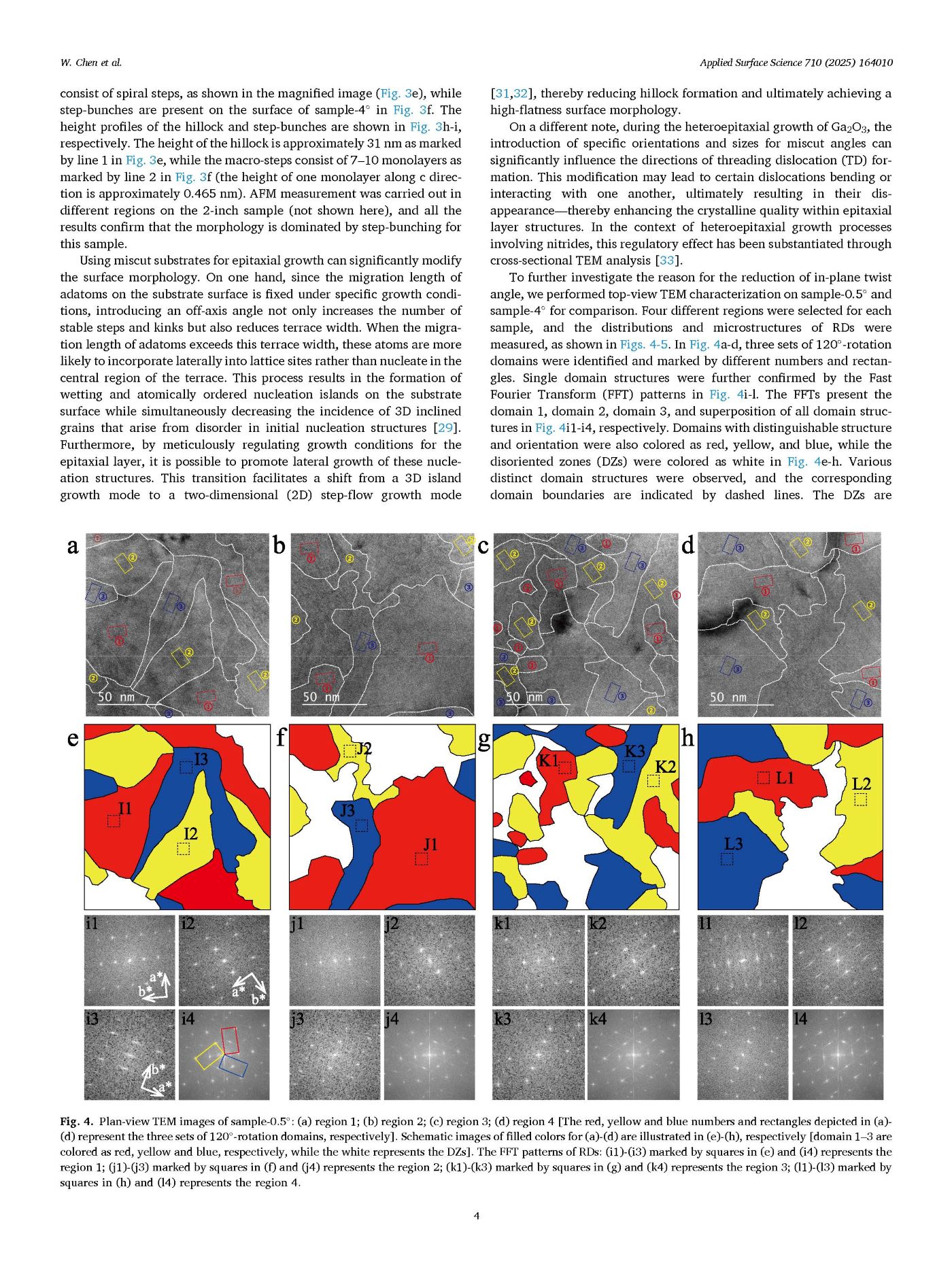
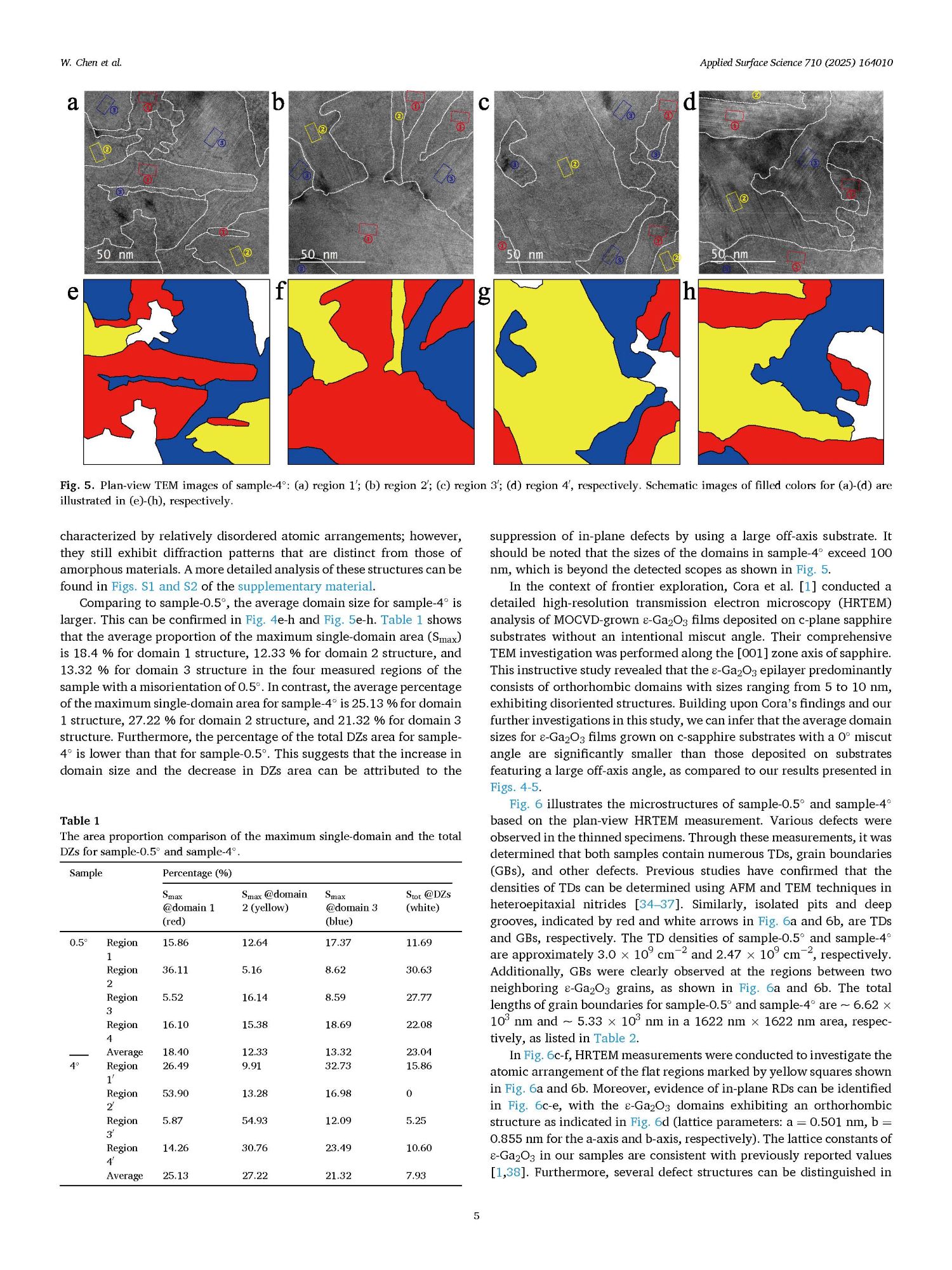
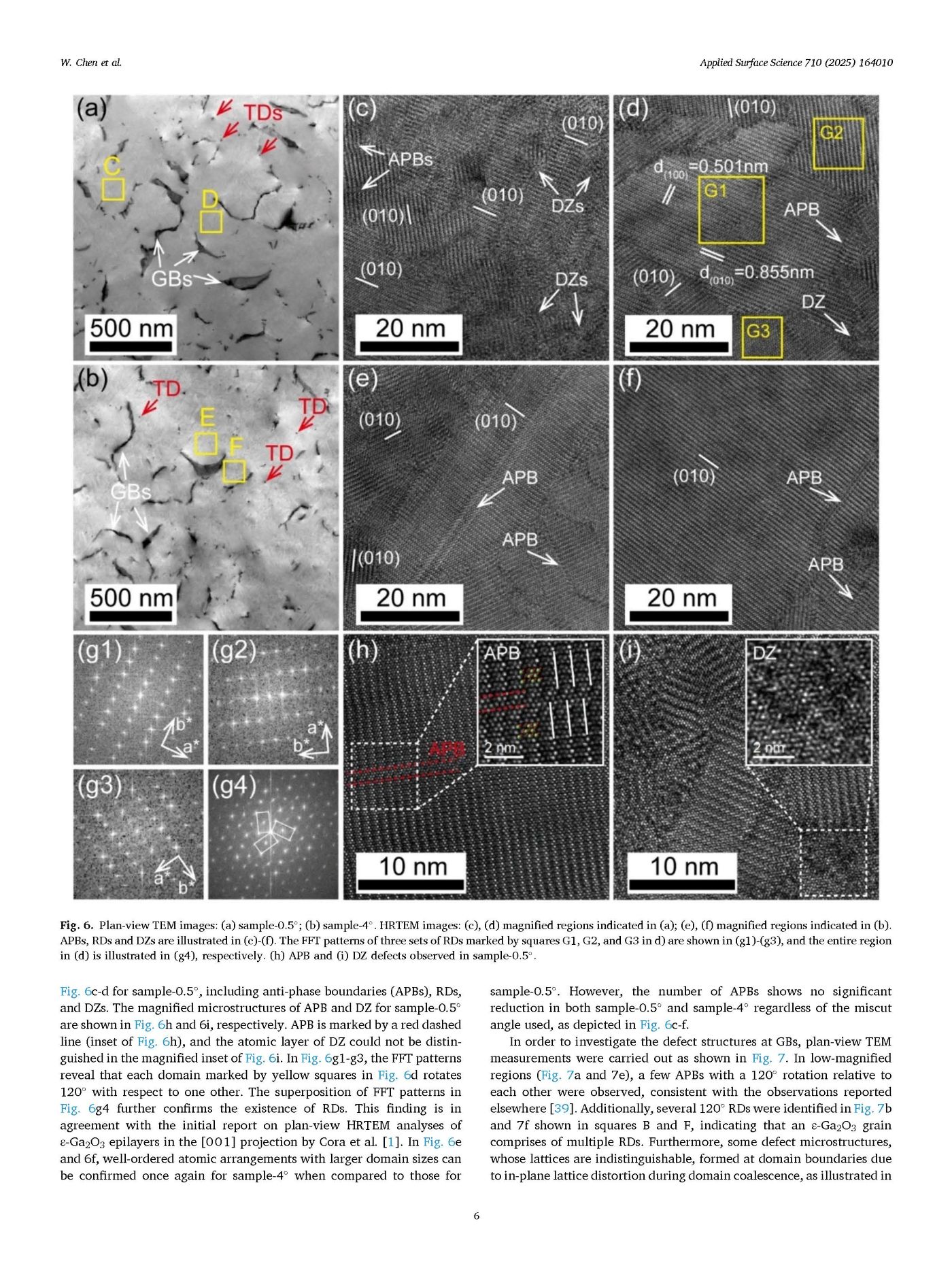
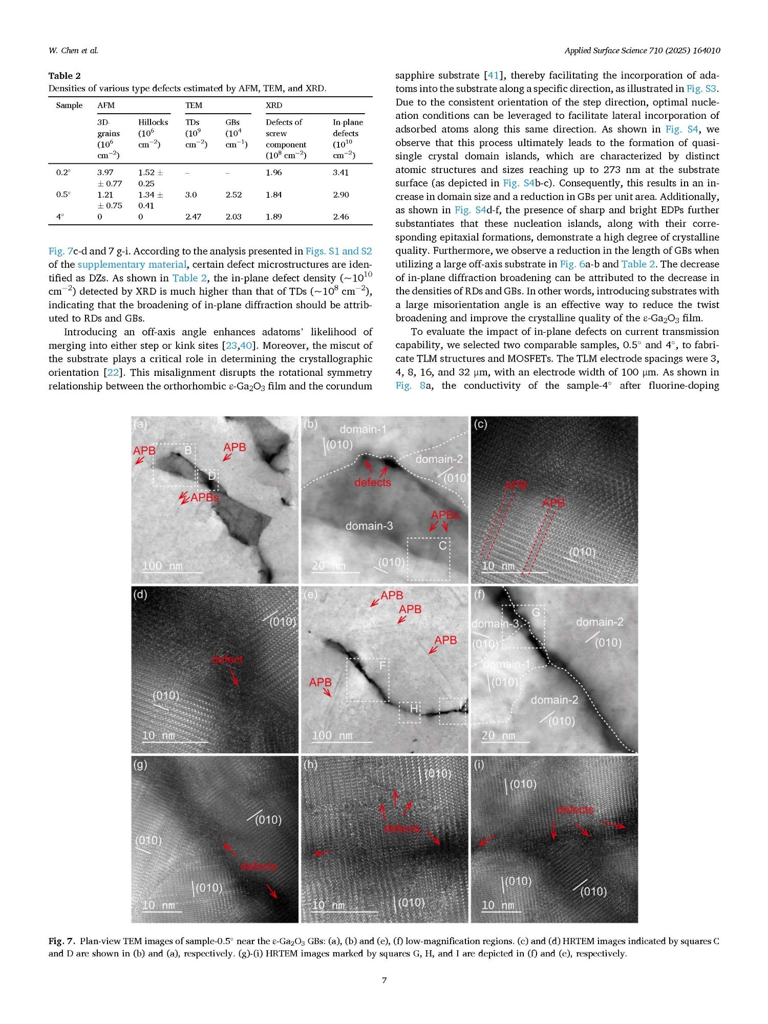
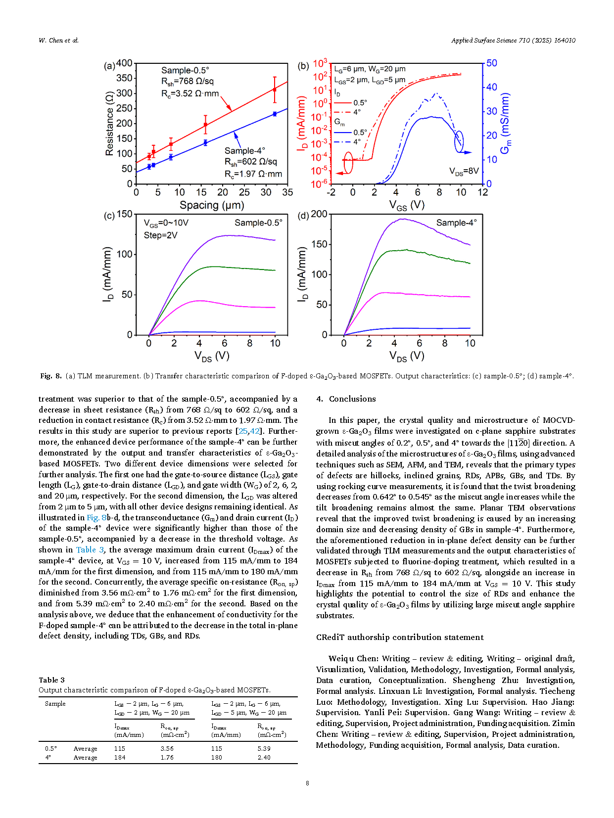
In this paper, the crystal quality and microstructure of MOCVD grown ε-Ga2O3 films were investigated on c-plane sapphire substrates with miscut angles of 0.2◦, 0.5◦, and 4◦ towards the [11-20] direction. A detailed analysis of the microstructures of ε-Ga2O3 films, using advanced techniques such as SEM, AFM, and TEM, reveals that the primary types of defects are hillocks, inclined grains, RDs, APBs, GBs, and TDs. By using rocking curve measurements, it is found that the twist broadening decreases from 0.642◦ to 0.545◦ as the miscut angle increases while the tilt broadening remains almost the same. Planar TEM observations reveal that the improved twist broadening is caused by an increasing domain size and decreasing density of GBs in sample-4◦. Furthermore, the aforementioned reduction in in-plane defect density can be further validated through TLM measurements and the output characteristics of MOSFETs subjected to fluorine-doping treatment, which resulted in a decrease in Rsh from 768 Ω/sq to 602 Ω/sq, alongside an increase in IDmax from 115 mA/mm to 184 mA/mm at VGS = 10 V. This study highlights the potential to control the size of RDs and enhance the crystal quality.
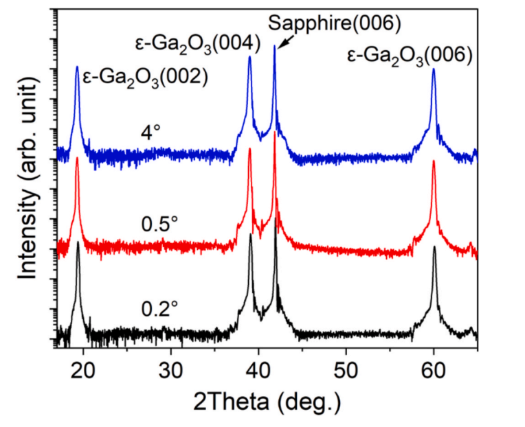
Fig. 1. 2θ-ω profiles of ε-Ga2O3 samples grown on 0.2◦, 0.5◦ and 4◦ misoriented c-plane sapphire substrates with the same growth parameters.
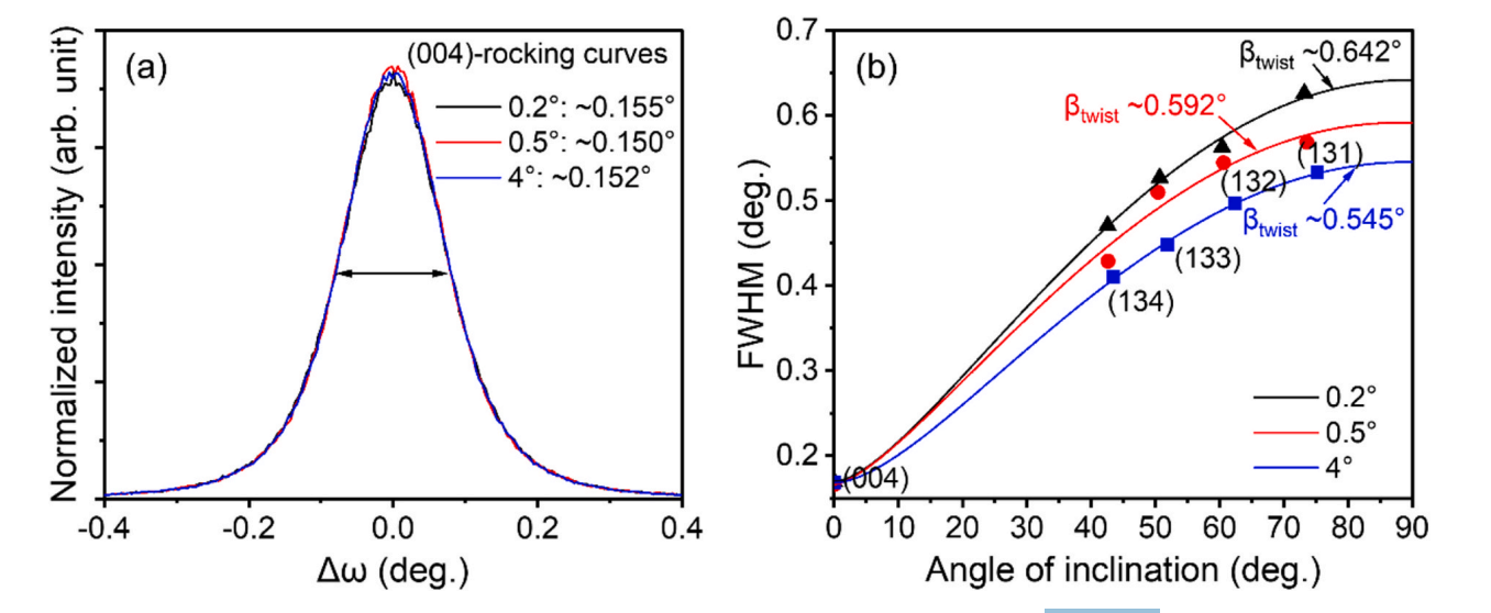
Fig. 2. Crystalline quality comparison: (a) (004)-plane rocking curves; (b) twist angles.
DOI:
doi.org/10.1016/j.apsusc.2025.164010