Paper Sharing
【International Papers】Achieving 0.05 Ω-mm contact resistance in non-alloyed Ti/Au ohmics to β-Ga₂O₃ by removing surface carbon
日期:2025-07-25阅读:474
Researchers from the Cornell University have published a dissertation titled "Achieving 0.05 Ω-mm contact resistance in non-alloyed Ti/Au ohmics to β-Ga2O3 by removing surface carbon" in APL Materials.
Background
Since the first demonstration in 2012, β-Ga2O3 transistors have been extensively investigated toward commercialization. Although Si currently dominates the transistor market, higher bandgap semiconductors offer superior critical electric field tolerance for more efficient high-power devices. SiC and GaN were the first wide-bandgap semiconductors to achieve commercial success. β-Ga2O3’s bandgap (4.8 eV) is greater than those of both SiC (3.3 eV) and GaN (3.4 eV), setting a higher theoretical limit to the Baliga figure of merit, which describes the fundamental trade-off in power electronics between breakdown voltage and device on resistance. β-Ga2O3 is also an economically viable and commercially scalable technology, due to the availability of melt-grown native substrates. Doping densities up to 5 × 1020 cm−3 have been demonstrated through various intrinsic and extrinsic doping methods for both channel and selective-area contact regions.
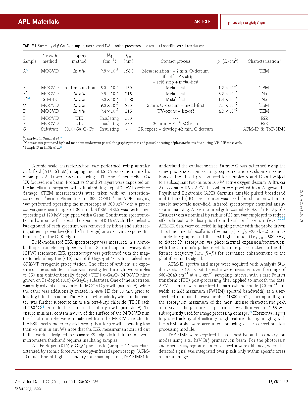
In this work, we correlate the ohmic behavior of non-annealed Ti/Au contacts on heavily doped (010) β-Ga2O3 with its interface structure and chemistry. Scanning transmission electron microscopy (STEM), atomic force microscopy-infrared spectroscopy (AFM-IR), and time-of-flight secondary ion mass spectra (ToF-SIMS) measurements reveal that carbon contamination can persist after the removal of photoresist patterns, inhibiting electrical conduction in the conventional lift-off fabrication process. We further show that ambient carbon contamination can be measured by electron energy loss spectroscopy (EELS) and electron spin resonance (ESR) spectroscopy and increases the contact resistance in a metal-first process that does not use photoresist. We demonstrate that sufficient cleaning of the Ga2O3 surface by UV-ozone or oxygen plasma descum achieves low-resistance contacts.
Abstract
Preserving a contamination-free metal–semiconductor interface in β-Ga2O3 is critical to achieve consistently low resistance (< 1 Ω-mm) ohmic contacts. Here, we report a scanning transmission electron microscopy study on the variation in Ti/Au ohmic contact quality to (010) β-Ga2O3 in a conventional lift-off vs a metal-first process. We observe a thin ∼1 nm carbon barrier between the Ti and Ga2O3 in a non-conductive contact fabricated by a conventional lift-off process, which we attribute to photoresist residue, not previously detected by x-ray photoelectron spectroscopy due to the thinness and patchy coverage of the carbon layer, as well as roughness of the Ga2O3 surface. This thin carbon barrier is confirmed by electron energy loss spectroscopy and atomic force microscopy-infrared spectroscopy. We believe that the presence of the thin and patchy carbon layer leads to the highly inconsistent contact behavior in previous reports on non-alloyed contacts. Adventitious carbon is also observed in a conductive ohmic contact metal-first processing on an as-grown sample. We find that a five minute active oxygen descum is sufficient to remove this carbon on as-grown samples, further improving the ohmic behavior and reducing the contact resistance Rc to 0.06 Ω-mm. We also show that an hour long UV-ozone treatment of the Ga2O3 surface can eliminate carbon residue from the lift-off processing, resulting in a low Rc of 0.05 Ω-mm.
Summary
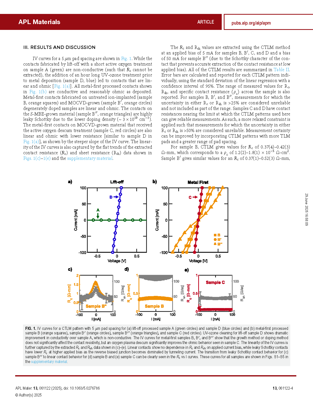
Overall, the variation in Ti/Au ohmic contact quality as a function of lift-off and metal-first processing has been investigated. STEM-EELS measurements find that the level of carbon contamination at the Ga2O3/Ti interface correlates directly with the measured ohmic contact resistance. We find non-conductive contacts fabricated by a lift-off process to contain significant photoresist carbon residue and hypothesize that the large variations in contact performance previously reported result from similar remnant photoresist. We further report that an hour-long UV-ozone treatment is shown to remove the photoresist residue to attain linear ohmic contacts with a contact resistance Rc of 0.05 Ω-mm. We propose that AFM-IR can be used as a non-destructive scanning probe measurement for mid-process diagnostic to ensure surface cleanliness prior to contact deposition for critical device processes. On the other hand, metal-first processing shows linear ohmic non-alloyed contact behavior on an as-grown sample. However, the contact interface still contains a carbon EELS signature from organic contamination due to air exposure that can also be detected by ESR spectroscopy. Addition of a 5 min active oxygen descum on the as-grown surface prior to contact metal deposition eliminates this adventitious carbon and results in a ∼5× reduction in contact resistance to 0.06 Ω-mm, the second lowest reported contact resistance to (010) β-Ga2O3 to date. We conclude that non-alloyed contacts are attainable via both lift-off and metal-first contact processing when surface carbon is managed appropriately.
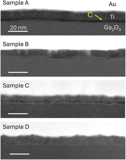
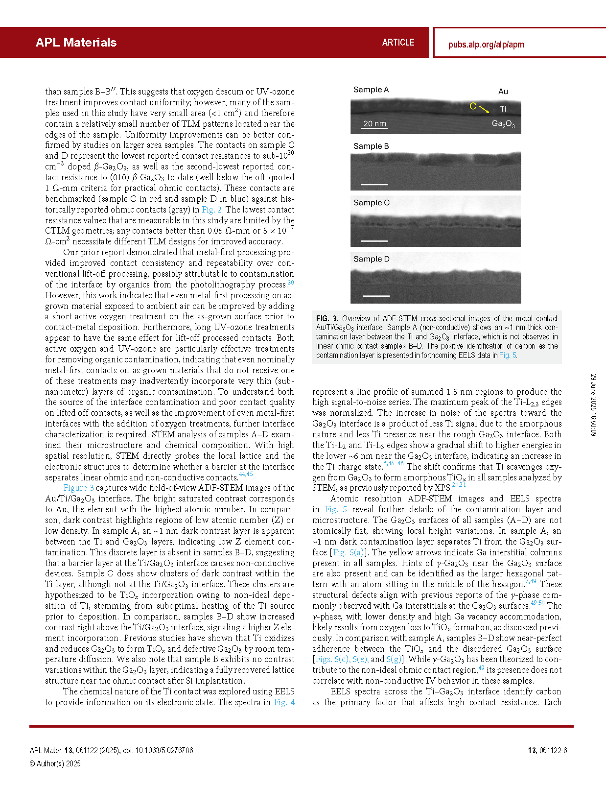
FIG. 1. Overview of ADF-STEM cross-sectional images of the metal contact Au/Ti/Ga2O3 interface. Sample A (non-conductive) shows an ∼1 nm thick contamination layer between the Ti and Ga2O3 interface, which is not observed in linear ohmic contact samples B–D.
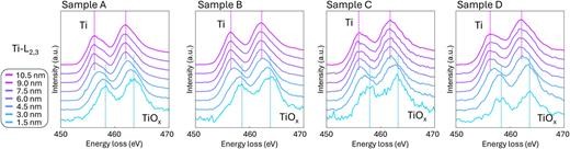
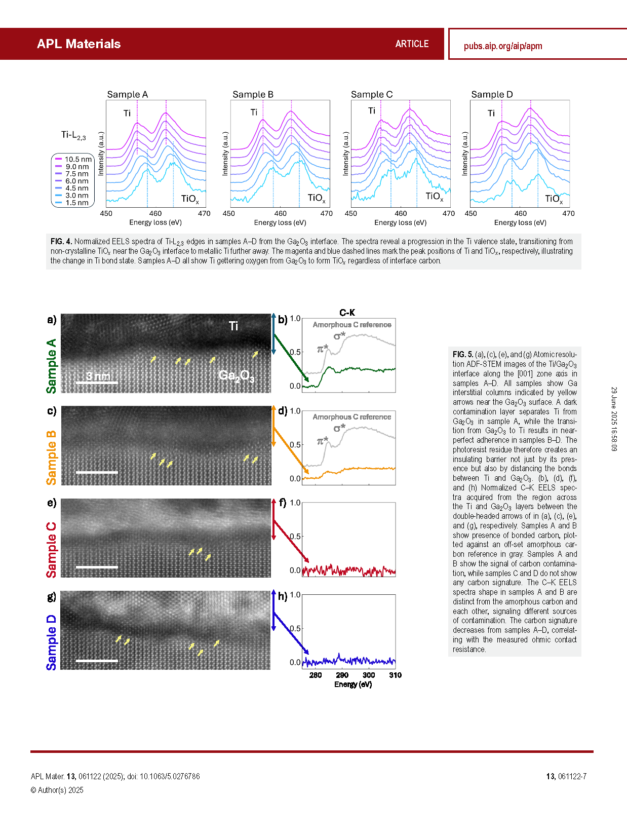
FIG. 2. Normalized EELS spectra of Ti-L2,3 edges in samples A–D from the Ga2O3 interface. The spectra reveal a progression in the Ti valence state, transitioning from non-crystalline TiOx near the Ga2O3 interface to metallic Ti further away. The magenta and blue dashed lines mark the peak positions of Ti and TiOx, respectively, illustrating the change in Ti bond state. Samples A–D all show Ti gettering oxygen from Ga2O3 to form TiOx regardless of interface carbon.
DOI:
doi.org/10.1063/5.0276786