Paper Sharing
【Domestic Papers】Fabrication and Ultraviolet Response Characteristics of All-Oxide Bi₂O₃/Ga₂O₃ Heterojunction
日期:2025-07-23阅读:474
Researchers from the Guangxi Minzu University have published a dissertation titled "Fabrication and Ultraviolet Response Characteristics of All-Oxide Bi2O3/Ga2O3 Heterojunction" in Crystals.
Project Support
The work is supported by Science and Technology Development Program of GuangXi (Grant No. GuiKe AD23026169), Natural Science Key Project in Scientific Research Foundation for Universities of Education Department of Anhui Province (Grant No. 2024AH051896), Startup Foundation for Doctoral Scientific Research of Wannan Medical College (Grant No. WYRCQD2023021), and National Natural Science Foundation of China (Grant No. 51862031).
Background
The fundamental mechanisms of heterojunction devices mainly rely on the band structures and carrier transport properties of different semiconductor materials, which contributes to their widespread use in high-speed switching devices, solar cells, photodetectors, and more. For heterojunction photodetectors, due to the differing energy band structures of the two materials, band bending and interfacial charge distribution are formed, leading to the generation of a built-in electric field. When suitable light illuminates the heterojunction photodetectors, photons are absorbed by the semiconductor, generating electron-hole pairs. Under the influence of a built-in electric field, the carriers transport in opposite directions, reach the electrode, and form a photocurrent. The inherent characteristics of heterojunctions enable heterojunction photodetectors to achieve high photoresponse performance, such as fast response, high gain, and even self-powering capabilities. Ultraviolet (UV) photodetectors as one important type of photodetectors have attracted tremendous attention due to the demand for missile tracking, scientific analysis, ozone hole monitoring, flame detecting, and so on. Recently, wide-bandgap semiconductor materials have emerged as a promising choice and present rapidly development in UV detection. Among the heterojunction UV photodetectors, type I (stradding) band alignments are usually constructed to improve the carrier separation efficiency.
Abstract
Heterojunctions are commonly used in optoelectronic devices to improve device performance. However, interface defects and lattice mismatch often hinder carrier transport and reduce efficiency, emphasizing the need for further exploration of diverse heterojunction structures. In this study, a heterojunction device constructed from Bi2O3 and Ga2O3 is demonstrated. The microstructures and photoelectrical properties of Bi2O3 and Ga2O3 thin films were investigated. Bi2O3 and Ga2O3 thin films show a bandgap of 3.19 and 5.10 eV. The Bi2O3/Ga2O3 heterojunction-based device demonstrates rectification characteristics, with a rectification ratio of 2.72 × 10³ at ±4.5 V and an ON/OFF ratio of 1.07 × 10⁵ (4.5/−3.9 V). Additionally, we fabricated a sandwich-structured photodetector based on the Bi2O3/Ga2O3 heterojunction and investigated its ultraviolet photoresponse performance. The photodetector exhibits low dark current (0.34 pA @ −3.9 V) and fast response rise/fall time (<40/920 ms). This work offers important perspectives on the advancement of large-area, low-cost, and high-speed Bi2O3 film-based heterojunction photodetectors.
Conclusions
In summary, all-oxide heterojunction and its UV response performance based on magnetron-sputtering-grown Bi2O3 and Ga2O3 thin films were reported. The structural characterization reveals α phase Bi2O3 and Ga2O3 shows polycrystalline structures. Furthermore, the Bi2O3/Ga2O3 heterojunction shows the highest ON/OFF ratio of 1.07 × 10⁷, and the photodetector shows a high PDCR of 2.11 × 10⁴ and a fast response speed of <40 ms rise time and 920 ms fall time. It is shown that Bi2O3/Ga2O3 heterojunction has potential for application in UV detection.
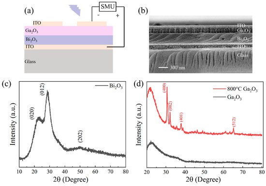
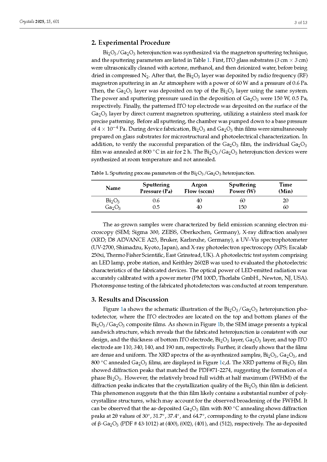
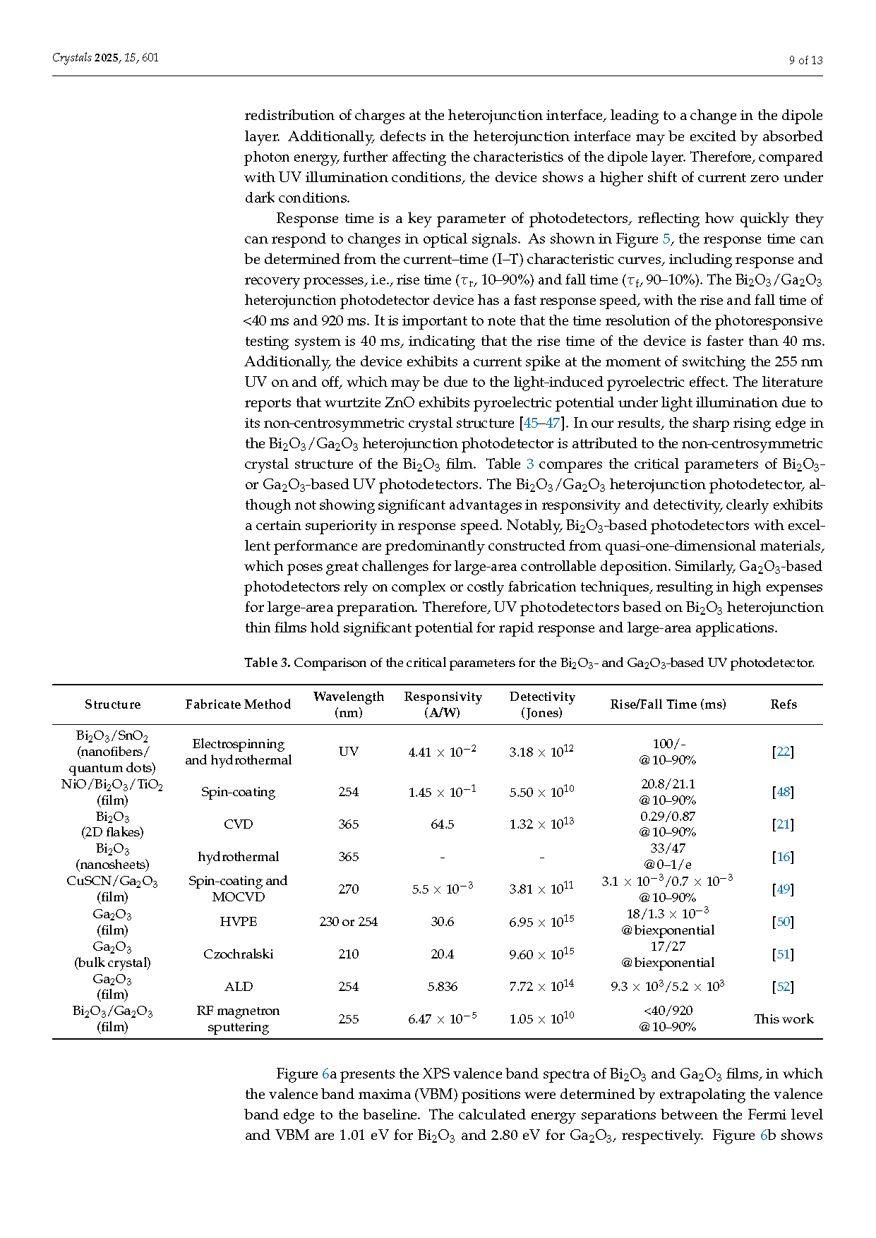
Figure 1. (a) The schematic illustration of the Bi2O3/Ga2O3 heterojunction and its UV response testing schematic. (b) The cross-section SEM image of the fabricated heterojunction. The XRD pattern of the as-deposited Bi2O3 film (c) and Ga2O3 film (d).
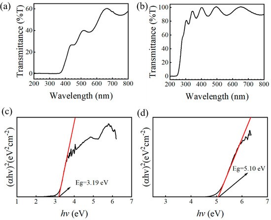
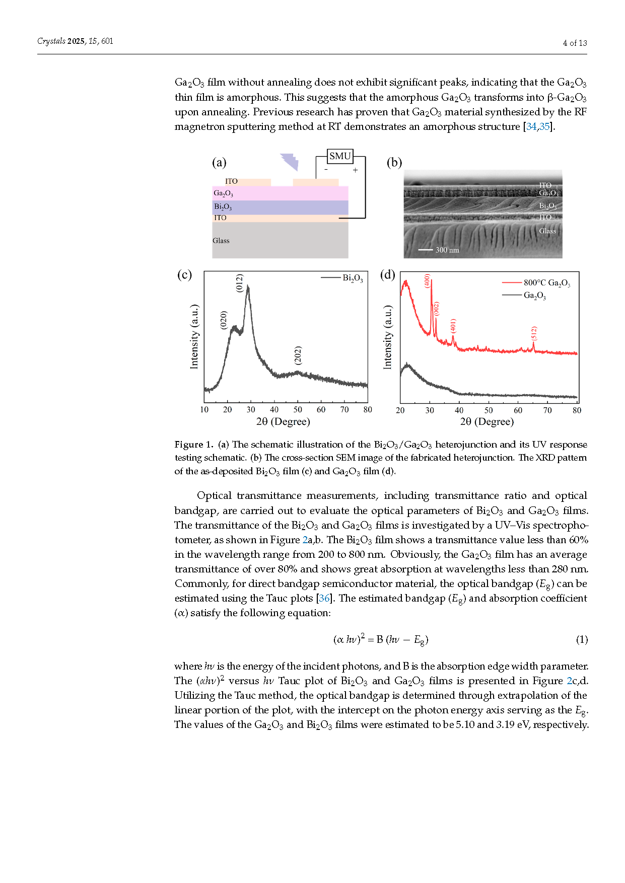
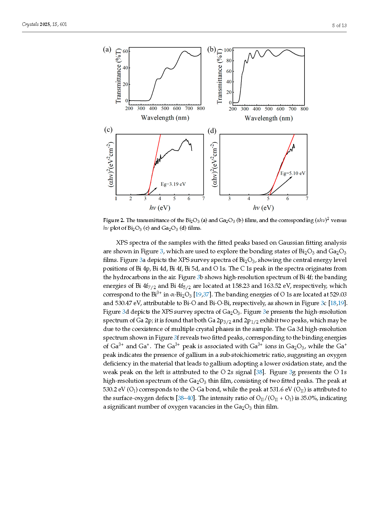
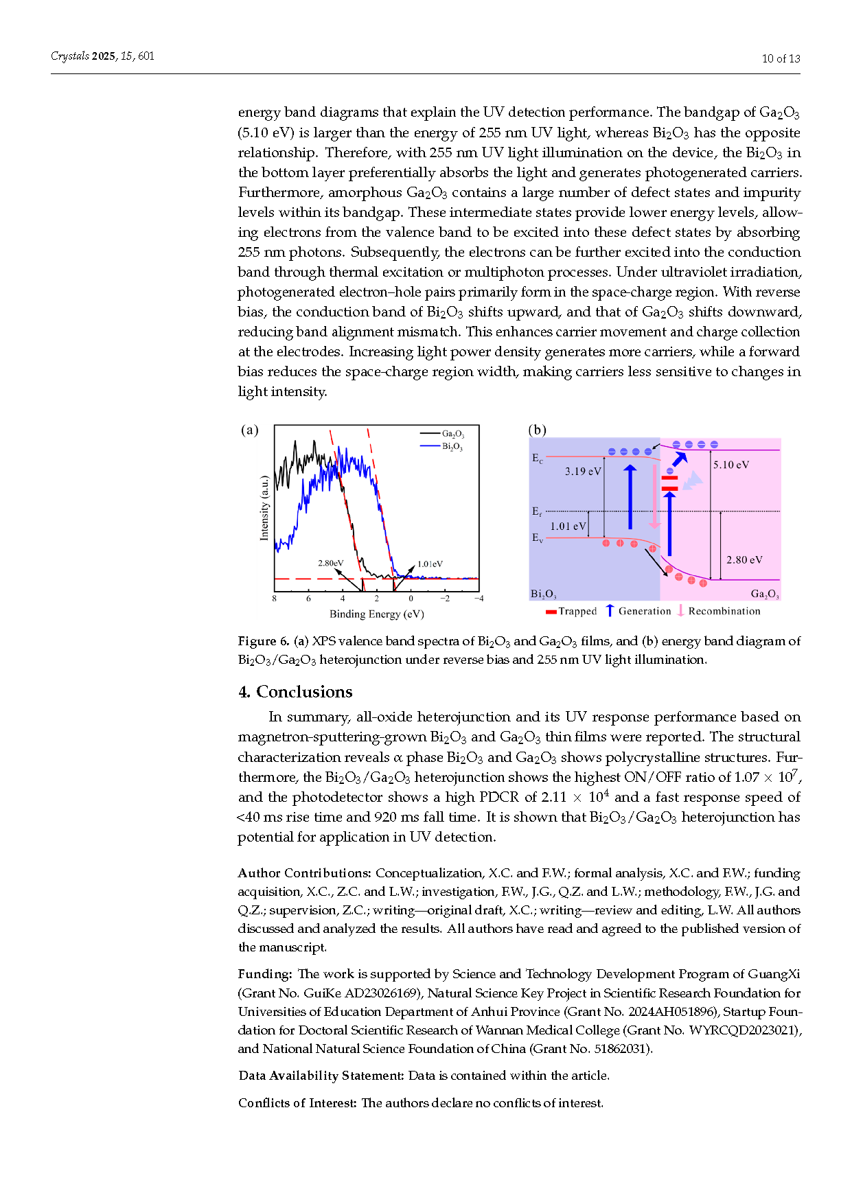
Figure 2. The transmittance of the Bi2O3 (a) and Ga2O3 (b) films, and the corresponding (αhν)2 versus hν plot of Bi2O3 (c) and Ga2O3 (d) films.
DOI:
doi.org/10.3390/cryst15070601