Paper Sharing
【International Papers】Self-Powered Ultraviolet-C Imaging Using Epitaxial Gallium Oxide Membranes with Anisotropic Domain Conduction
日期:2025-07-23阅读:456
Researchers from the Seoul National University have published a dissertation titled "Self-Powered Ultraviolet-C Imaging Using Epitaxial Gallium Oxide Membranes with Anisotropic Domain Conduction" in ACS Nano.
Abstract
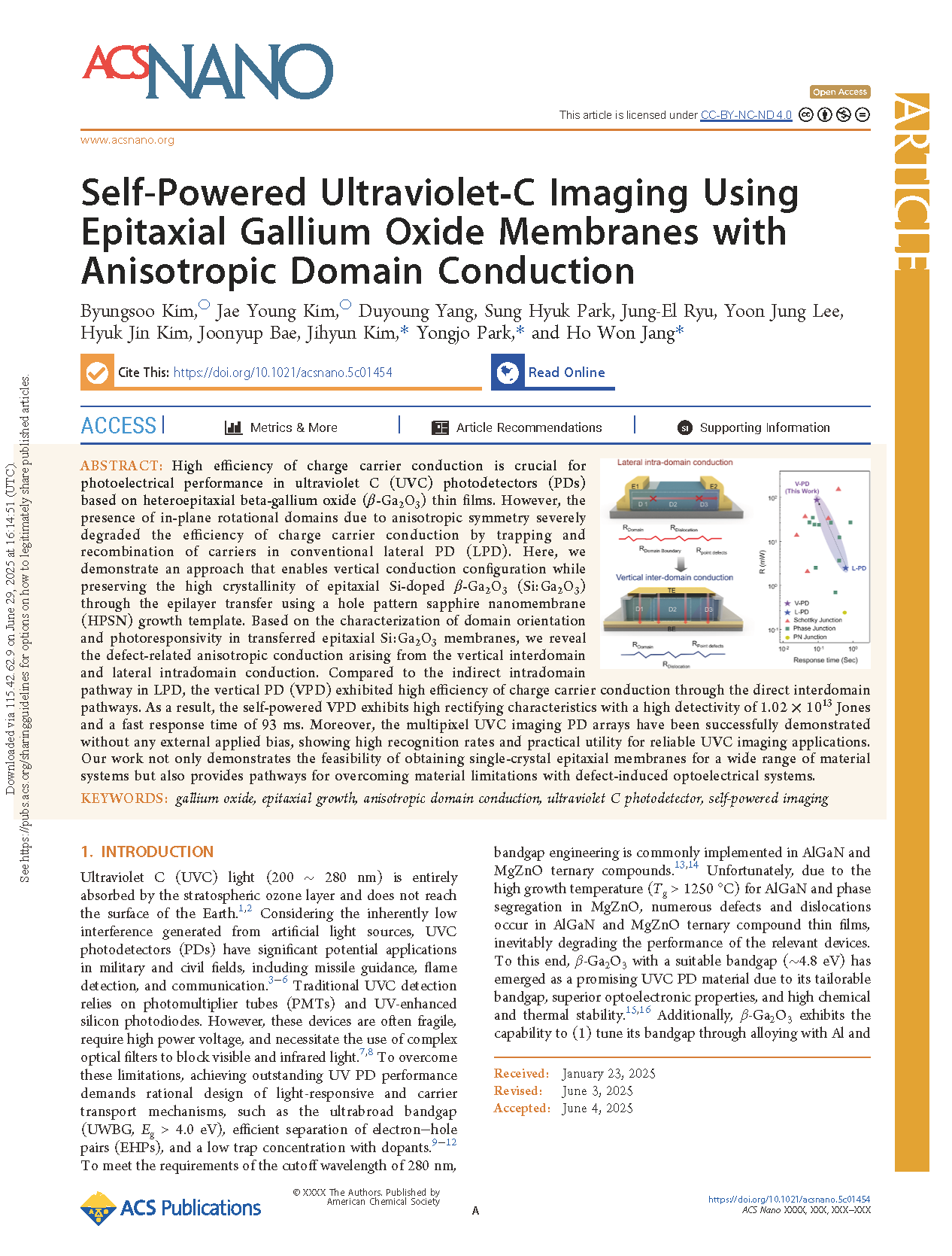
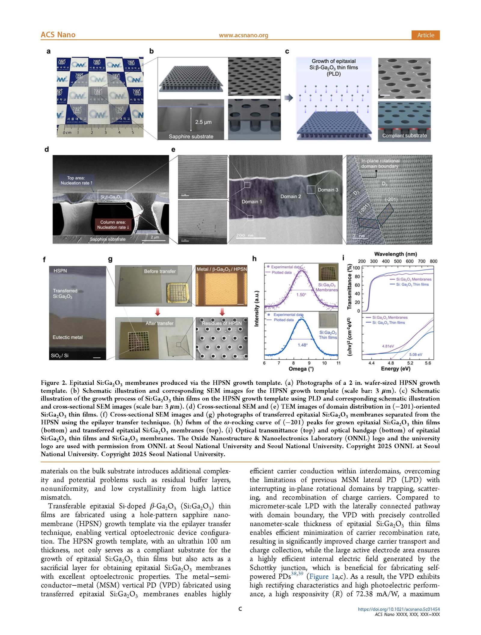
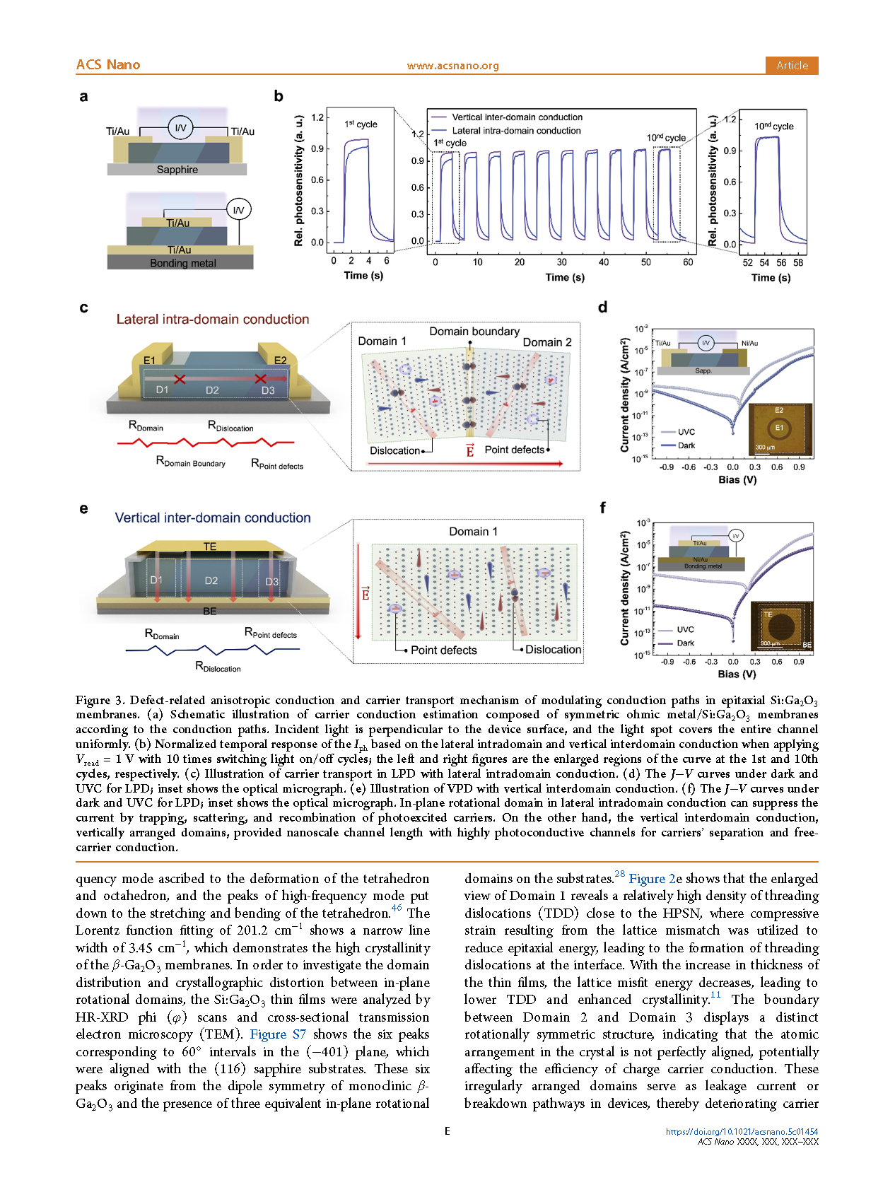
High efficiency of charge carrier conduction is crucial for photoelectrical performance in ultraviolet C (UVC) photodetectors (PDs) based on heteroepitaxial beta-gallium oxide (β-Ga2O3) thin films. However, the presence of in-plane rotational domains due to anisotropic symmetry severely degraded the efficiency of charge carrier conduction by trapping and recombination of carriers in conventional lateral PD (LPD). Here, we demonstrate an approach that enables vertical conduction configuration while preserving the high crystallinity of epitaxial Si-doped β-Ga2O3 (Si:Ga2O3) through the epilayer transfer using a hole pattern sapphire nanomembrane (HPSN) growth template. Based on the characterization of domain orientation and photoresponsivity in transferred epitaxial Si:Ga2O3 membranes, we reveal the defect-related anisotropic conduction arising from the vertical interdomain and lateral intradomain conduction. Compared to the indirect intradomain pathway in LPD, the vertical PD (VPD) exhibited high efficiency of charge carrier conduction through the direct interdomain pathways. As a result, the self-powered VPD exhibits high rectifying characteristics with a high detectivity of 1.02 × 10¹³ Jones and a fast response time of 93 ms. Moreover, the multipixel UVC imaging PD arrays have been successfully demonstrated without any external applied bias, showing high recognition rates and practical utility for reliable UVC imaging applications. Our work not only demonstrates the feasibility of obtaining single-crystal epitaxial membranes for a wide range of material systems but also provides pathways for overcoming material limitations with defect-induced optoelectrical systems.
Conclusion
In this study, we successfully demonstrated epitaxial Si:Ga2O3 membranes for multipixel self-powered UVC PD arrays. The epitaxial Si:Ga2O3 membranes were fabricated by epilayer transfer using an HPSN growth template with an ultrathin 100 nm-thick substrate. Based on the defect-related anisotropy conduction in epitaxial Si:Ga2O3 membranes, we demonstrated VPD showing a high responsivity of 72.38 mA/W and a fast response time of 93 ms at 0 V bias, which is attributed to the vertical interdomain conduction for efficient carrier conduction and photoconductive nanometer-scale pathways for suppressing recombination of charge carriers at domain boundaries. Furthermore, the multipixel UVC imaging PD arrays were successfully demonstrated for light-imaging applications without the need for an external power supply. This work presents an innovative strategy for achieving high-quality epitaxial Si:Ga2O3 membranes with modulated conduction paths and paves the way for Ga2O3 heterogeneous integrated optoelectronic technology.
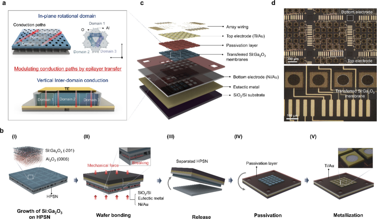
Figure 1. 5 × 5 self-powered UVC imaging PD arrays based on epitaxial Si:Ga2O3 membranes. (a) Strategy to overcome the in-plane rotational domain that causes lateral intradomain conduction, which exhibits a low efficiency of carrier separation, by modulating conduction paths through the epilayer transfer technique. (b) Schematic illustration depicting the fabrication procedure for UVC imaging PD arrays. Demonstrating a vertical structure PD by transferring epitaxial Si:Ga2O3 thin films using the HPSN growth template. (c) Schematic structure of 5 × 5 pixelated UVC PD arrays. (d) OM image of multipixel UVC PD arrays and enlarged images of PD in devices.

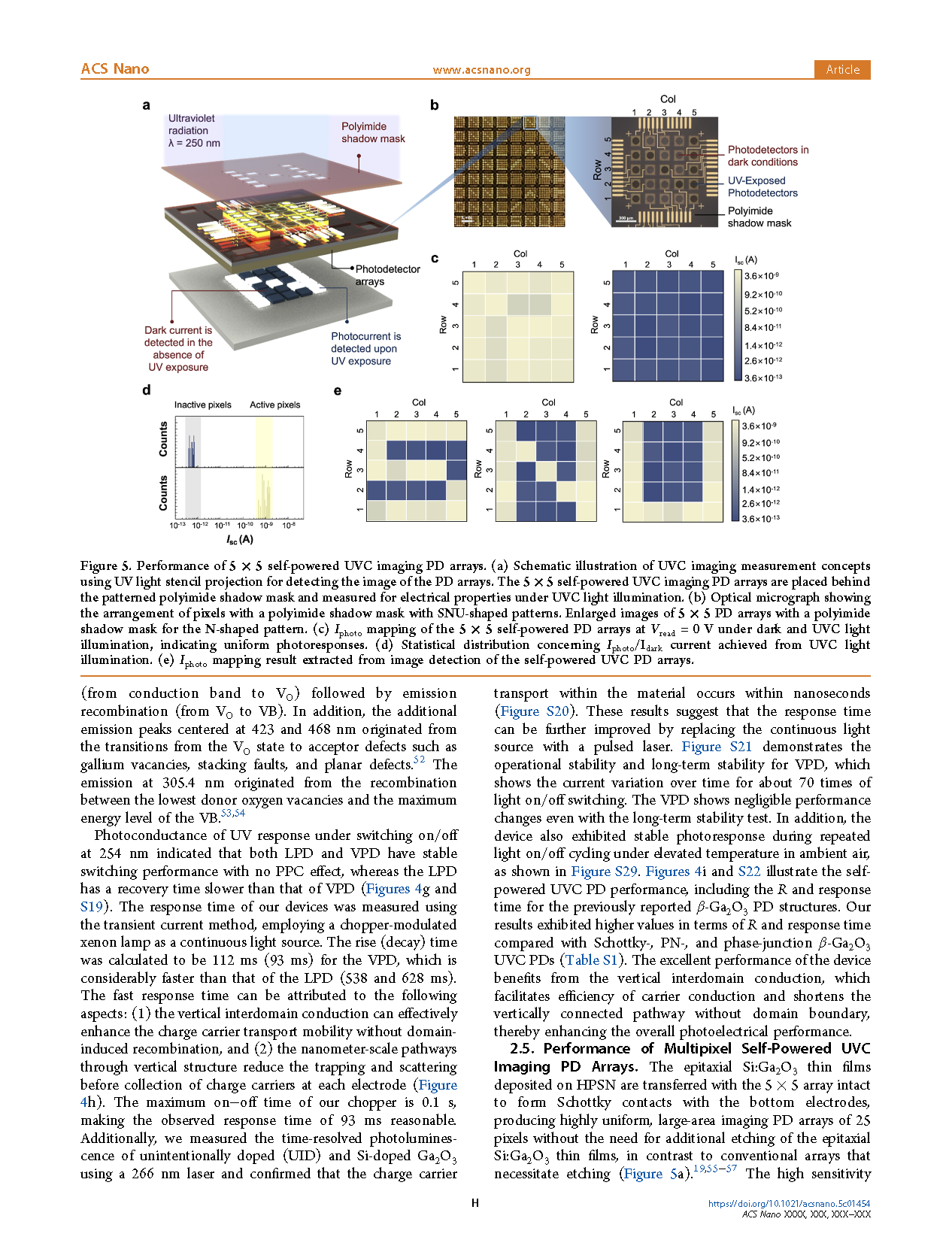
Figure 2. Performance of 5 × 5 self-powered UVC imaging PD arrays. (a) Schematic illustration of UVC imaging measurement concepts using UV light stencil projection for detecting the image of the PD arrays. The 5 × 5 self-powered UVC imaging PD arrays are placed behind the patterned polyimide shadow mask and measured for electrical properties under UVC light illumination. (b) Optical micrograph showing the arrangement of pixels with a polyimide shadow mask with SNU-shaped patterns. Enlarged images of 5 × 5 PD arrays with a polyimide shadow mask for the N-shaped pattern. (c) Iphoto mapping of the 5 × 5 self-powered PD arrays at Vread = 0 V under dark and UVC light illumination, indicating uniform photoresponses. (d) Statistical distribution concerning Iphoto/Idark current achieved from UVC light illumination. (e) Iphoto mapping result extracted from image detection of the self-powered UVC PD arrays.
DOI:
doi.org/10.1021/acsnano.5c01454