Paper Sharing
【International Papers】Single-phase κ-Ga₂O₃ films deposited by metal-organic chemical vapor deposition on GaAs and ternary BₓGa(₁₋ₓ)As templates
日期:2025-07-04阅读:521
Researchers from the University of Parma have published a dissertation titled "Single-phase κ-Ga2O3 films deposited by metal-organic chemical vapor deposition on GaAs and ternary BxGa(1-x)As templates" in Applied Surface Science.
Background
In the field of deep ultraviolet (UV) photonics and power electronic devices there is an increasing interest in sesquioxide materials with a bandgap that ranges from 2.9 eV for cubic In2O3 (bixbyite structure) to 8.9 eV for hexagonal Al2O3. Ga2O3 is a prominent member of this family, known to have five polymorphs, namely: α, β, γ, δ and κ. The monoclinic β-Ga2O3 is the most studied phase because it is thermodynamically stable and can be grown as bulk single crystal, epilayer, and nanostructures. β-Ga2O3 has a substantially higher breakdown electric field (6–8 MV/cm) than silicon, silicon carbide, and gallium nitride, which allows Ga2O3-based devices to work at higher voltages. Inherent drawbacks of the β polymorph are, however, its anisotropic physical characteristics, anisotropic thermal expansion coefficients, and easy cleavage. Because of that, the metastable κ-polymorph with orthorhombic crystal structure and bandgap of about 4.7 eV also received attention in recent years. When deposited on c-oriented sapphire substrates, it forms very small (lateral size 10–30 nm) domains separated by 120° twins, which ultimately give rise to a pseudo-hexagonal structure.
Abstract
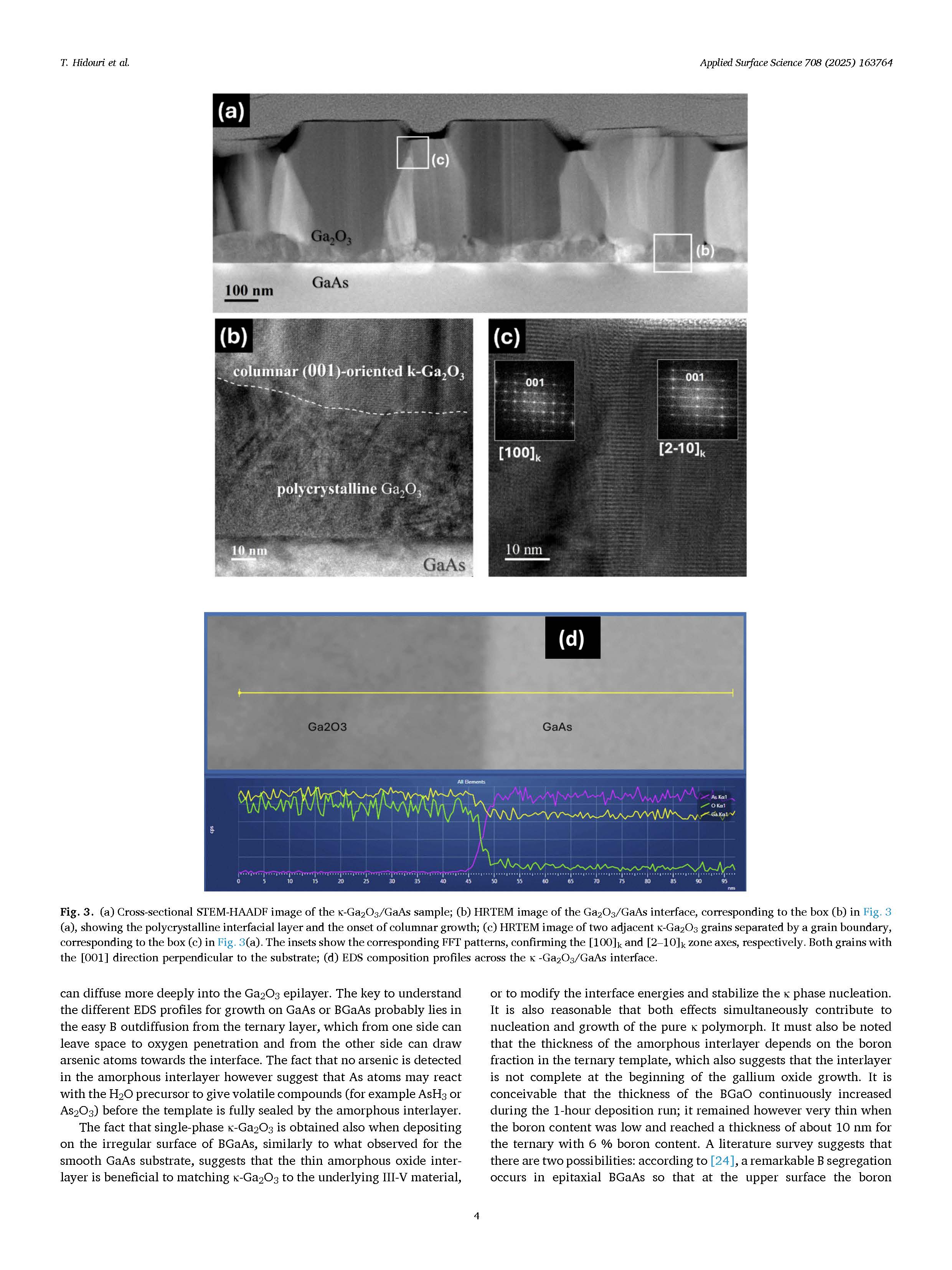
For the first time, single-phase κ-Ga2O3 films were grown on (001) p-type GaAs and BxGa(1-x)As /GaAs templates using Metal-Organic Chemical Vapor Deposition (MOCVD). The films were analyzed by X-ray diffraction (XRD), scanning electron microscopy (SEM), and transmission electron microscopy (TEM). TEM investigations revealed a thin polycrystalline nucleation layer followed by well-oriented columnar growth of the κ-phase in the Ga2O3/GaAs sample, while segregation and diffusion effects in the ternary alloy led to boron accumulation on the template surface, which reacted with oxygen during the first stage of Ga2O3 deposition to form a thin amorphous oxide (a-BGaO) at the interface between Ga2O3 and the BGaAs/GaAs template. Again, columnar growth of large [001]-oriented grains of the orthorhombic κ-phase occurred on the amorphous nucleation layers, which resulted in a compact gallium oxide film. These polycrystalline or amorphous interlayers are important as they provide a suitable platform for growth of phase-pure orthorhombic κ-Ga2O3 on III-V cubic substrates. This work paves the way to the integration of κ-Ga2O3 and III-V semiconductors, for preparing heterojunctions for novel electronic and optoelectronic devices.
Conclusions
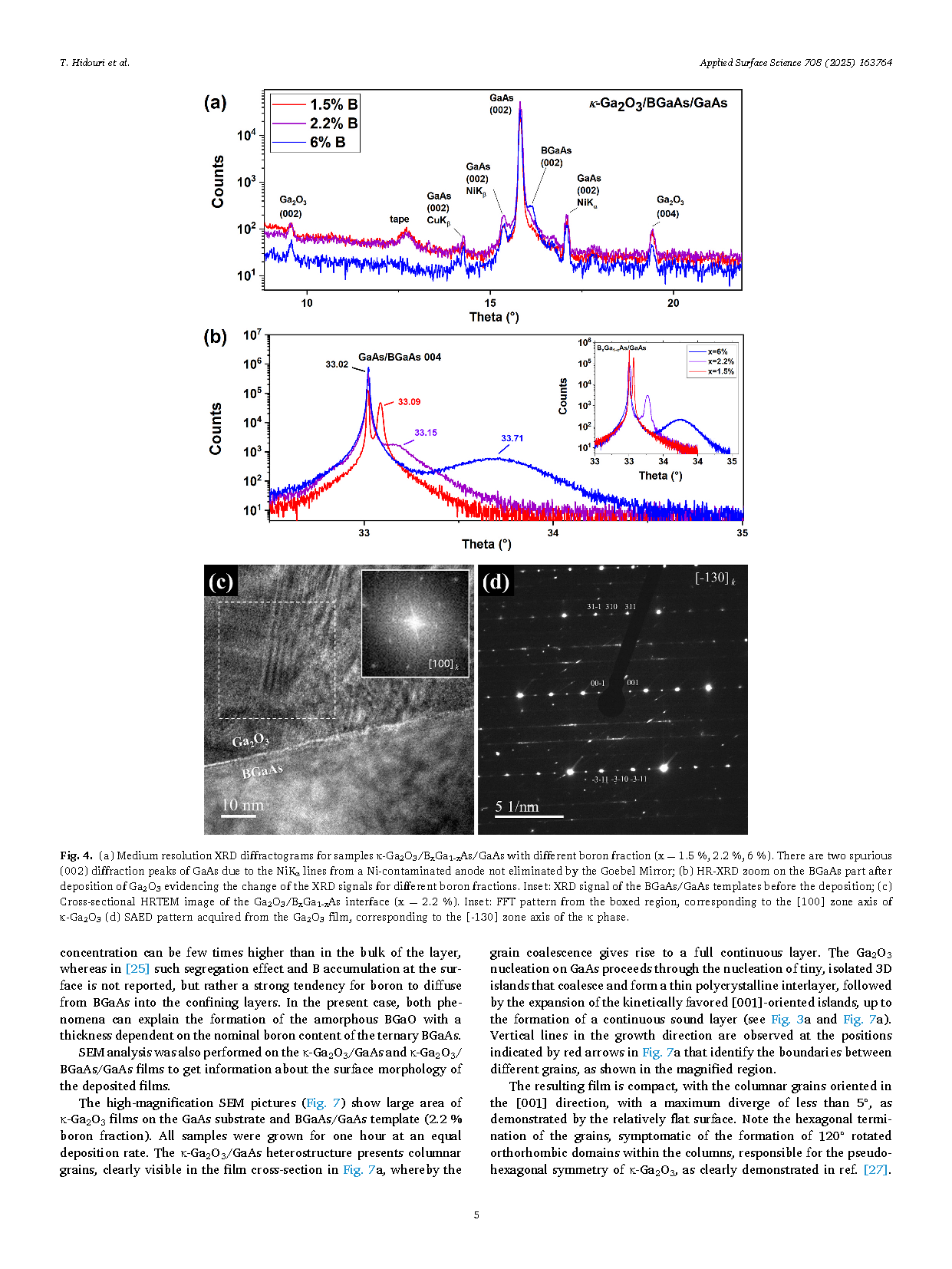
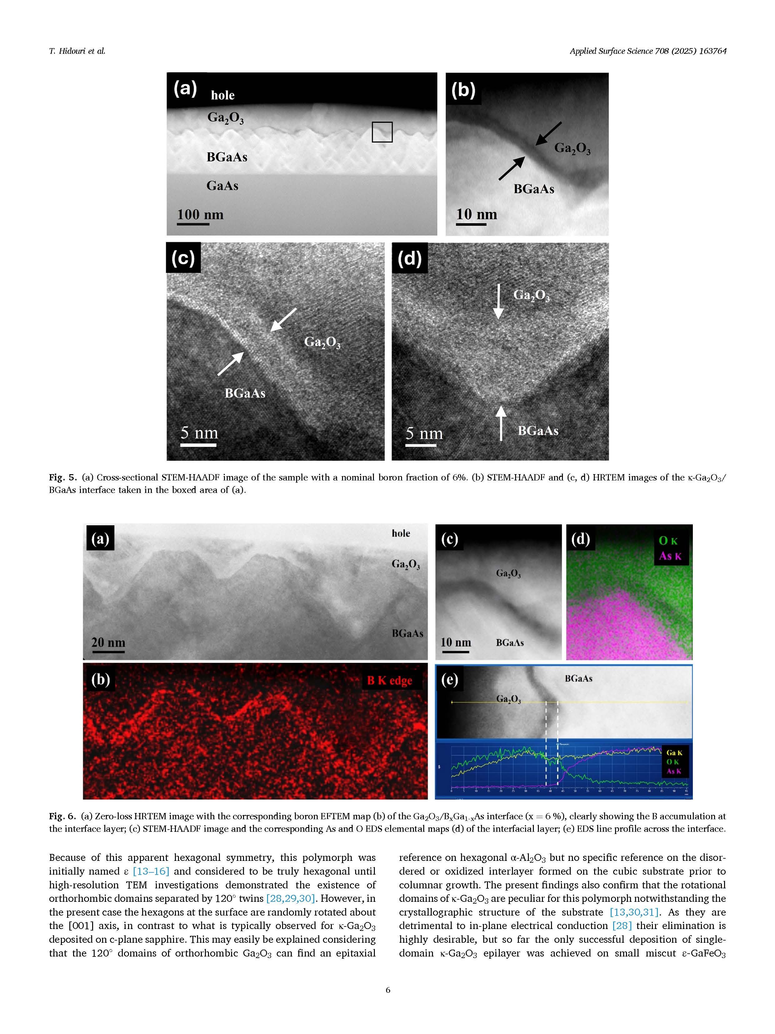
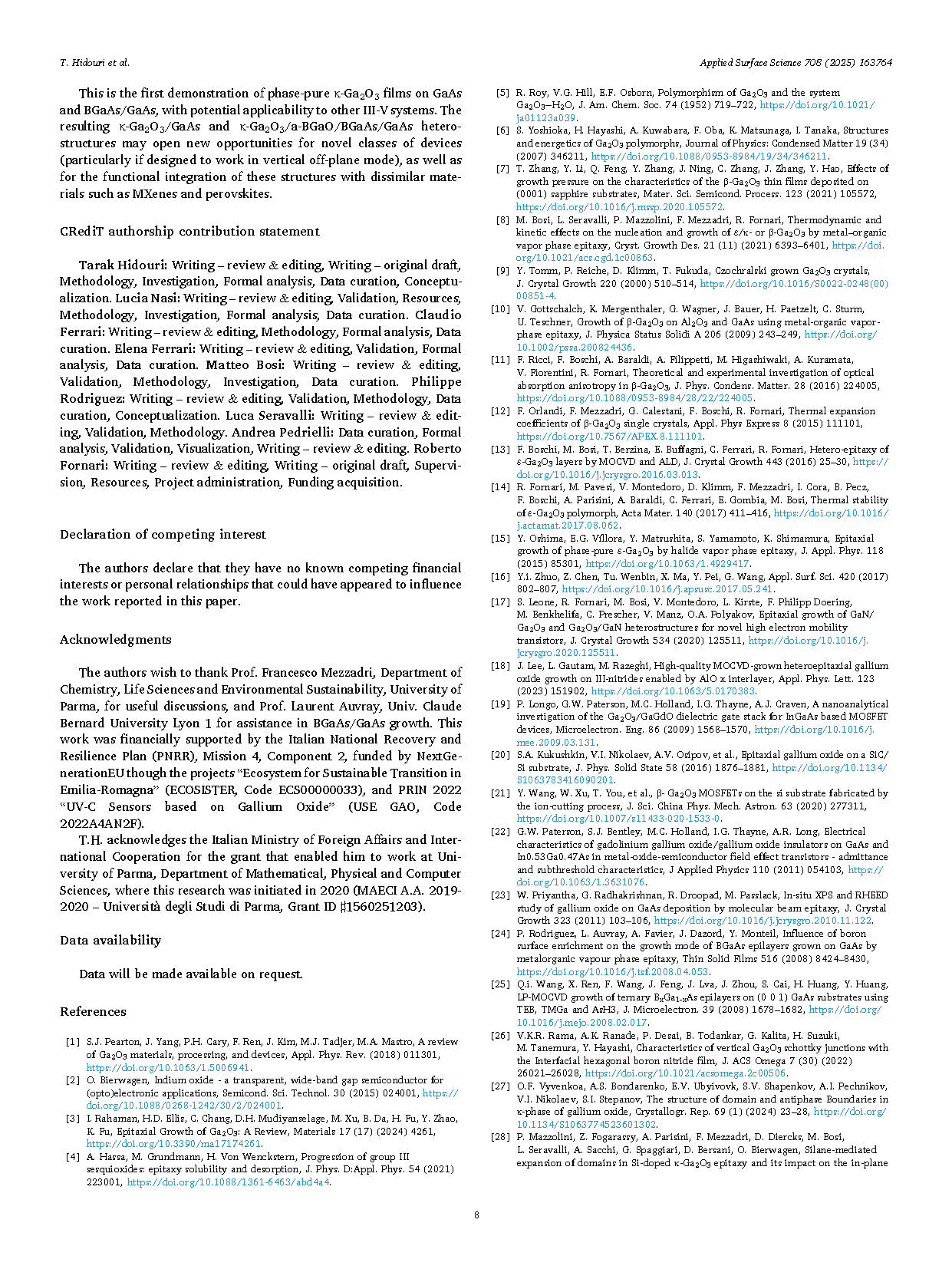
Phase-pure κ-Ga2O3 layers were grown by MOCVD on (001) p-type GaAs substrates and BGaAs/GaAs ternary alloy templates. Remarkably, in Ga2O3/GaAs, a thin polycrystalline nucleation layer forms at the interface with GaAs. It acts as strain relaxation buffer, enabling the subsequent κ-Ga2O3 film to develop along the [001] orientation, preferentially expanding and extending the grains with the (001) plane parallel to GaAs. This nucleation mechanism leads to formation of a continuous layer made of columnar [001]-oriented grains, satisfactorily aligned despite the lattice mismatch with GaAs. The result of deposition on BGaAs ternary templates is quite different, because the BGaAs surface is quite rough, with roughness depending on the B content. Furthermore, the boron atoms tend to accumulate at the surface of the ternary template, partly because of segregation during growth of the template itself, but also by virtue of the outdiffusion during the growth of Ga2O3 at T > 600 °C. The excess B at the template surface leads to the formation of a thin amorphous BGaO interlayer that follows the contour of the BGaAs surface. This amorphous interlayer seems to produce two major effects: it acts as platform for the Ga2O3 nucleation of larger islands (no polycrystalline nucleation layer was detected in this case) but the columnar grains have a different degree of tilt, so that the morphology of the film is worse than seen for the Ga2O3/GaAs structure. In both systems, the formation of an interfacial layer, either polycrystalline Ga2O3 or amorphous BGaO, appears to facilitate strain relaxation and partially decouple the growing film from the substrate during the early stages of growth. This promotes κ-phase stabilization and enables the development of a sound film with columnar [0 0 1]-oriented grains.
This is the first demonstration of phase-pure κ-Ga2O3 films on GaAs and BGaAs/GaAs, with potential applicability to other III-V systems. The resulting κ-Ga2O3/GaAs and κ-Ga2O3/a-BGaO/BGaAs/GaAs heterostructures may open new opportunities for novel classes of devices (particularly if designed to work in vertical off-plane mode), as well as for the functional integration of these structures with dissimilar materials such as MXenes and perovskites.
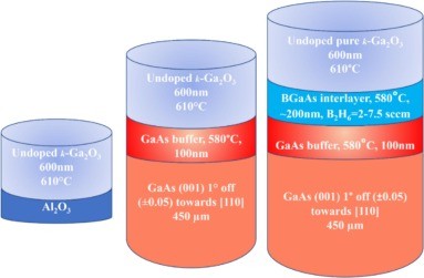
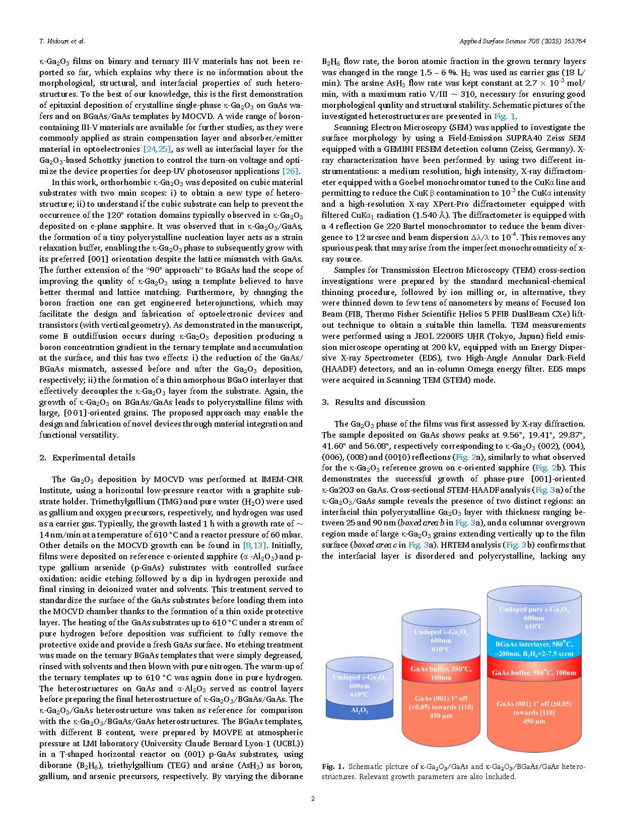
Fig. 1. Schematic picture of κ-Ga2O3/GaAs and κ-Ga2O3/BGaAs/GaAs heterostructures. Relevant growth parameters are also included.
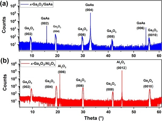
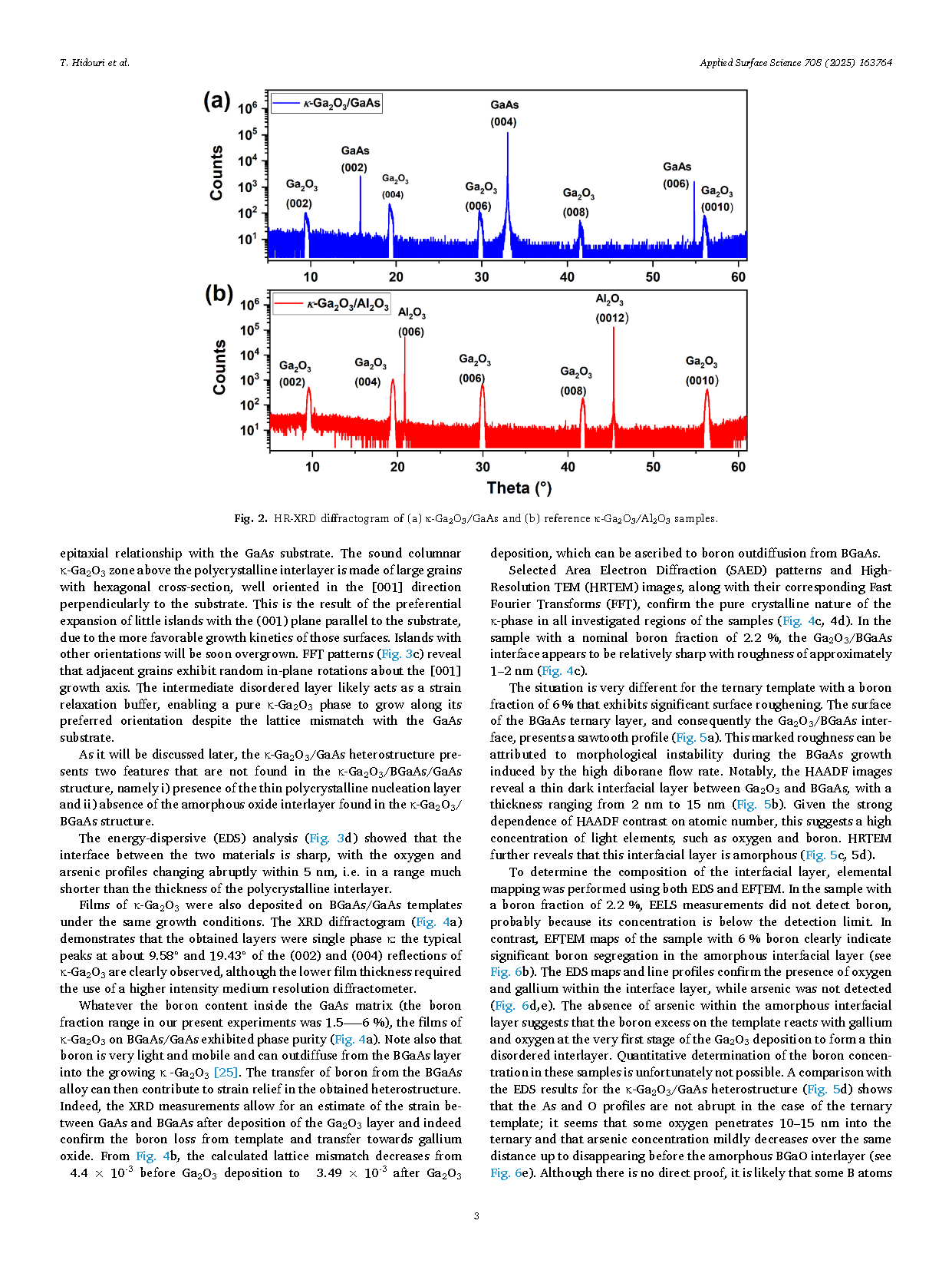
Fig. 2. HR-XRD diffractogram of (a) κ-Ga2O3/GaAs and (b) reference κ-Ga2O3/Al2O3 samples.
DOI:
doi.org/10.1016/j.apsusc.2025.163764