Paper Sharing
【International Papers】Comprehensive study of β-Ga₂O₃ epitaxial growth using a variable closed-coupled showerhead MOCVD reactor
日期:2025-06-05阅读:720
Researchers from the University of Texas at Austin have published a dissertation titled "Comprehensive study of β-Ga2O3 epitaxial growth using a variable closed-coupled showerhead MOCVD reactor" in Applied Physics Reviews.
Corresponding Author

Dr. Li received her B.S. degree form Peking University and Ph.D. degree from the University of California at Los Angeles. Following post-doctoral positions at California Institute of Technology and University of Illinois, as well as industry experience at II-VI, Inc. (formerly EpiWorks, Inc.), she joined the faculty of the University of Illinois, Urbana-Champaign (UIUC) in 2007. At UIUC, she was the Donald Biggar Willett Professor in Engineering and the interim director of the Nick Holonyak Jr. Micro and Nanotechnology Laboratory. She joined the faculty of UT in Aug. 2021. She holds the Temple Foundation Endowed Professorship No. 3 Professor in Department of Electrical and Computer Engineering. She also has an affiliate appointment in Chemistry as the Fellow of the Dow Professorship.
Her research focuses on nanostructured semiconductor materials and devices. She has published >160 journal papers and holds >20+ patents, delivered > 140 invited lectures worldwide. Her research opens new avenues by using innovative epitaxial growth and nanofabrication approaches including metalorganic chemical vapor deposition (MOCVD) of III-N and Ga2O3, metal-assisted chemical vapor deposition (MacEtch), and strain-induced self-rolled-up membranes (S-RuM), to address the ever-present needs to reduce the size, weight, power, and cost (SWAP-C) of microelectronic devices, among other applications.
Abstract
β-Ga2O3 is a highly promising ultrawide bandgap semiconductor material that is poised to transform the high-power electronics field. The manufacturability of device quality β-Ga2O3 epitaxial films at scale is urgently needed. Using a production-ready closed-coupled showerhead MOCVD reactor with in situ reflectance monitoring, this study presents a detailed investigation of the impact of growth parameters on the epitaxial growth of β-Ga2O3 on both (010) and (001) oriented native substrates, as well as on c-plane sapphire substrates with 0°–8° off-axis orientations. By tuning the showerhead–susceptor gap and mapping the other growth parameters, including annealing, nucleation, growth temperature, reactor pressure, and substrate orientation, we achieved state-of-the-art crystal quality, extraordinary wafer-level thickness uniformity of <1% variation for both 2-in. and 4-in. substrates for growth rates as high as 7.2 μm/h. All growth was performed using TMGa and pure O2 as the precursors and N2 as the carrier gas instead of the more widely used argon; no detectable nitrogen and carbon incorporation was observed by secondary ion mass spectrometry. For the homoepitaxy of Si-doped β-Ga2O3 films on (010) substrates, a room temperature Hall mobility of 148 cm2/V s was achieved at a carrier concentration of 1.26 × 1017 cm−3, with a growth rate of 2.6 μm/h. For the heteroepitaxy on sapphire, off-axis substrates exhibited enhanced crystallinity, as shown by the continued reduction of x-ray diffraction rocking curve full width at half maximum from 2834 to 1300 arcsec for 0° and 8° offcut sapphire substrates, respectively. The results demonstrate the scalability and potential advantages of this reactor design for manufacturing-scale β-Ga2O3 growth and offer new insights into the controllability of uniform high-quality films for power electronics applications.
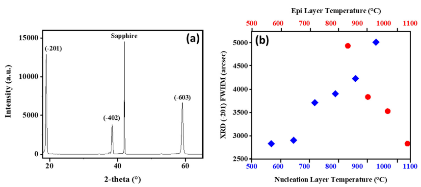
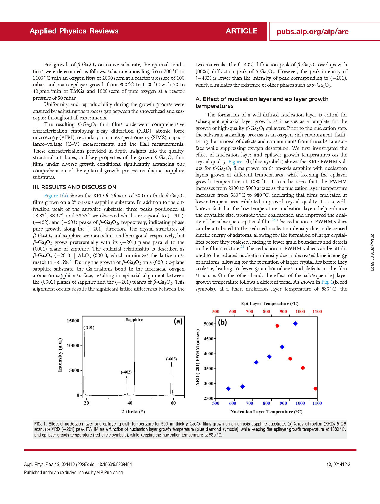
FIG. 1. Effect of nucleation layer and epilayer growth temperature for 500 nm thick β-Ga2O3 films grown on an on-axis sapphire substrate. (a) X-ray diffraction (XRD) θ–2θ scan, (b) XRD (-201) peak FWHM as a function of nucleation layer growth temperature (blue diamond symbols), while keeping the epilayer growth temperature at 1080°C, and epilayer growth temperature (red circle symbols), while keeping the nucleation temperature at 580°C.
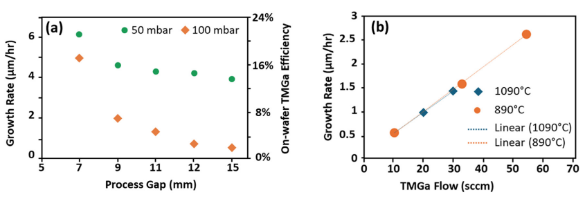
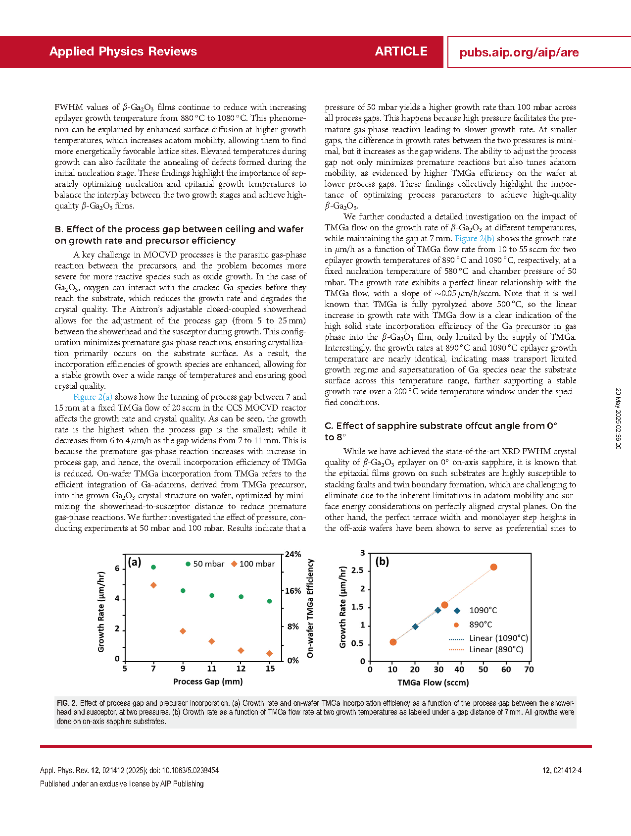
FIG. 2. Effect of process gap and precursor incorporation. (a) Growth rate and on-wafer TMGa incorporation efficiency as a function of the process gap between the showerhead and susceptor, at two pressures. (b) Growth rate as a function of TMGa flow rate at two growth temperatures as labeled under a gap distance of 7 mm. All growths were done on on-axis sapphire substrates.
DOI:
doi.org/10.1063/5.0239454