Paper Sharing
【International Papers】Tetravalent Element Doping of β-Ga₂O₃ Films Grown by Pulsed Electron Deposition Technique
日期:2025-05-23阅读:707
Researchers from the Institute of Materials for Electronics and Magnetism, CNR have published a dissertation titled " Tetravalent Element Doping of β-Ga2O3 Films Grown by Pulsed Electron Deposition Technique " in Journal of Alloys and Compounds.
Abstract
The Pulsed Electron Deposition (PED) technique was exploited to explore n-type doping of β-Ga2O3 thin films. Layers were deposited on (0001) sapphire at low-temperature (500°C), using homemade targets including variable amounts of Sn, Ge and Zr. The undoped films show a pure β-Ga2O3 phase with high crystallinity and an insulating nature, reporting resistivity values higher than 107 Ω cm. The introduction of Sn leads to the formation of films including both |- and β-Ga2O3, with an electrical resistivity of approximately 105 Ω cm. The doping with Ge results in the formation of high-quality β-Ga2O3 layers, but with high resistivity (~106 Ω cm). Zr is identified as the most effective dopant, resulting in the formation of single-phase epitaxial β-Ga2O3 films with low resistivity (~5 Ω cm). The present study indicates the PED technique to be an effective method for the deposition of good quality epitaxial β-Ga2O3 films at low temperatures, allowing the simple exploration of doping without the need for complex or toxic precursors.
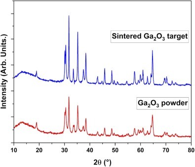
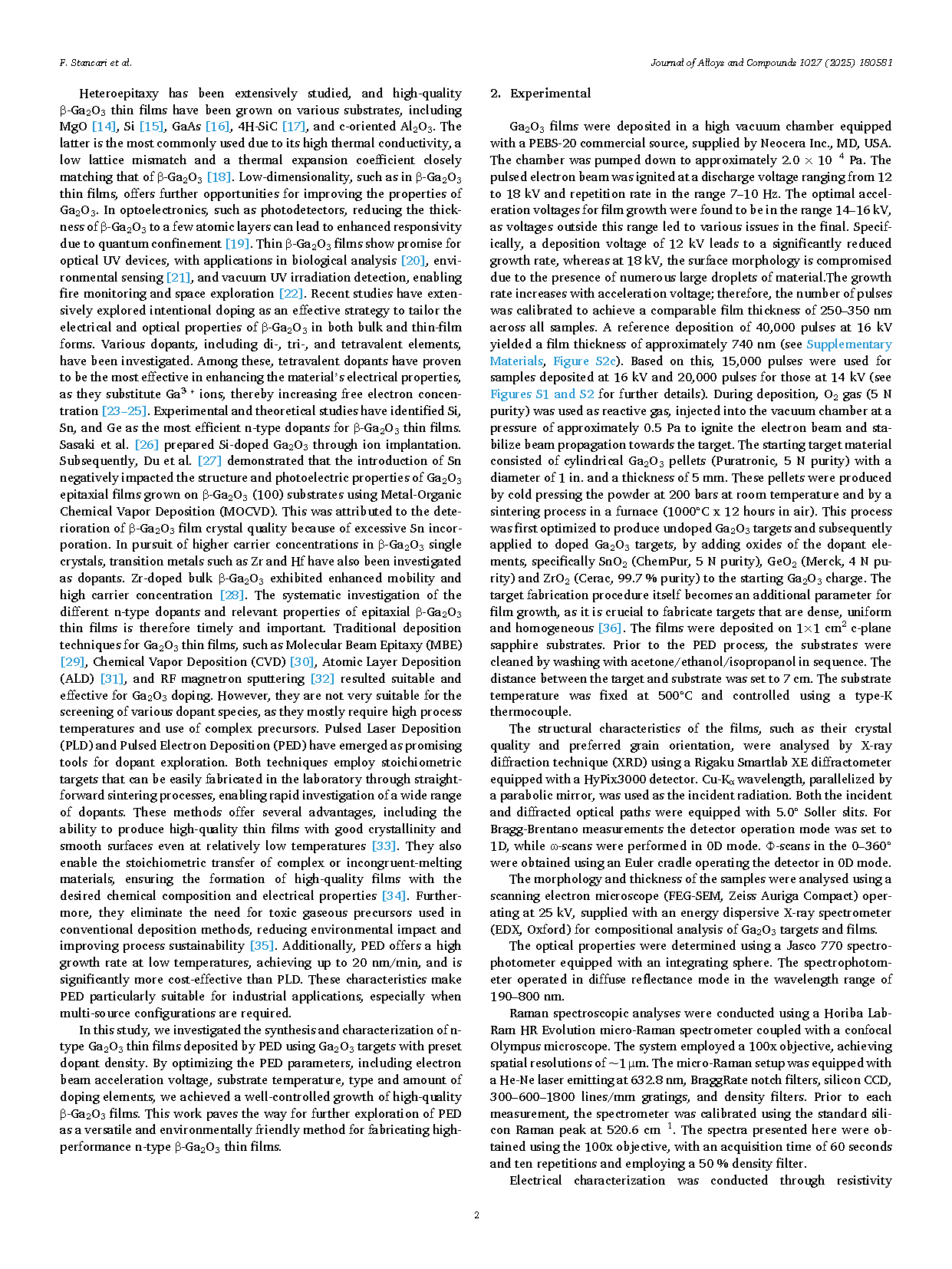
Fig. 1. XRD pattern of the initial Ga2O3 powder (red line) and of the sintered target (blue line).
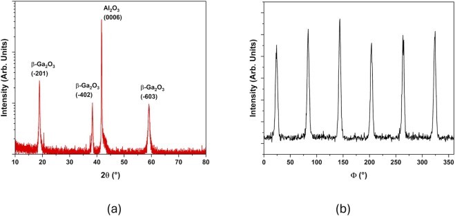
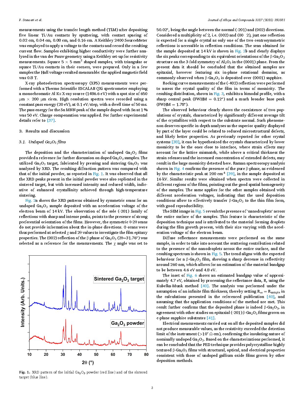
Fig. 2. XRD patterns (a) and Φ-scan (b) of a thin film deposited by PED at 14 kV starting from the undoped Ga2O3 target (red). XRD pattern intensity is reported in Log scale.
DOI:
doi.org/10.1016/j.jallcom.2025.180581