Paper Sharing
【Member Papers】Xidian University---High-performance gate-all-around phototransistor with a Ga₂O₃/NiO heterojunction for advanced ultraviolet detection
日期:2025-04-23阅读:695
Researchers from the Chongqing University of Posts and Telecommunications and Xidian University have published a dissertation titled "High-performance gate-all-around phototransistor with a Ga2O3/NiO heterojunction for advanced ultraviolet detection" in Applied Optics.
Project Support
China Postdoctoral Science Foundation (2023M742732); Postdoctoral Fellowship Program of China Postdoctoral Science Foundation (GZC20241303); Fundamental Research Funds for the Central Universities (XJSJ24100); National Natural Science Foundation of China (62404176).
Background
Solar-blind ultraviolet (UV) radiation (200–280 nm) plays a critical role in various applications such as environmental monitoring, flame detection, and missile tracking due to its complete absorption by stratospheric ozone, which eliminates natural background interference. For these applications, high sensitivity, low noise, and fast response are essential requirements for UV photodetectors. Traditional wide-bandgap semiconductors such as AlxGa1−xN and ZnxMg1−xO have been extensively explored for solar-blind UV detection, yet their practical applications face significant challenges. AlxGa1−xN requires extremely high growth temperatures for Al-rich compositions, while ZnxMg1−xO suffers from material degradation caused by heavy Mg doping. Other materials, like GaN and diamond, are constrained by their narrower bandgap or difficulties in large-area fabrication. These limitations necessitate the development of alternative materials and device architectures to achieve reliable and high-performance solar-blind UV detection.
Abstract
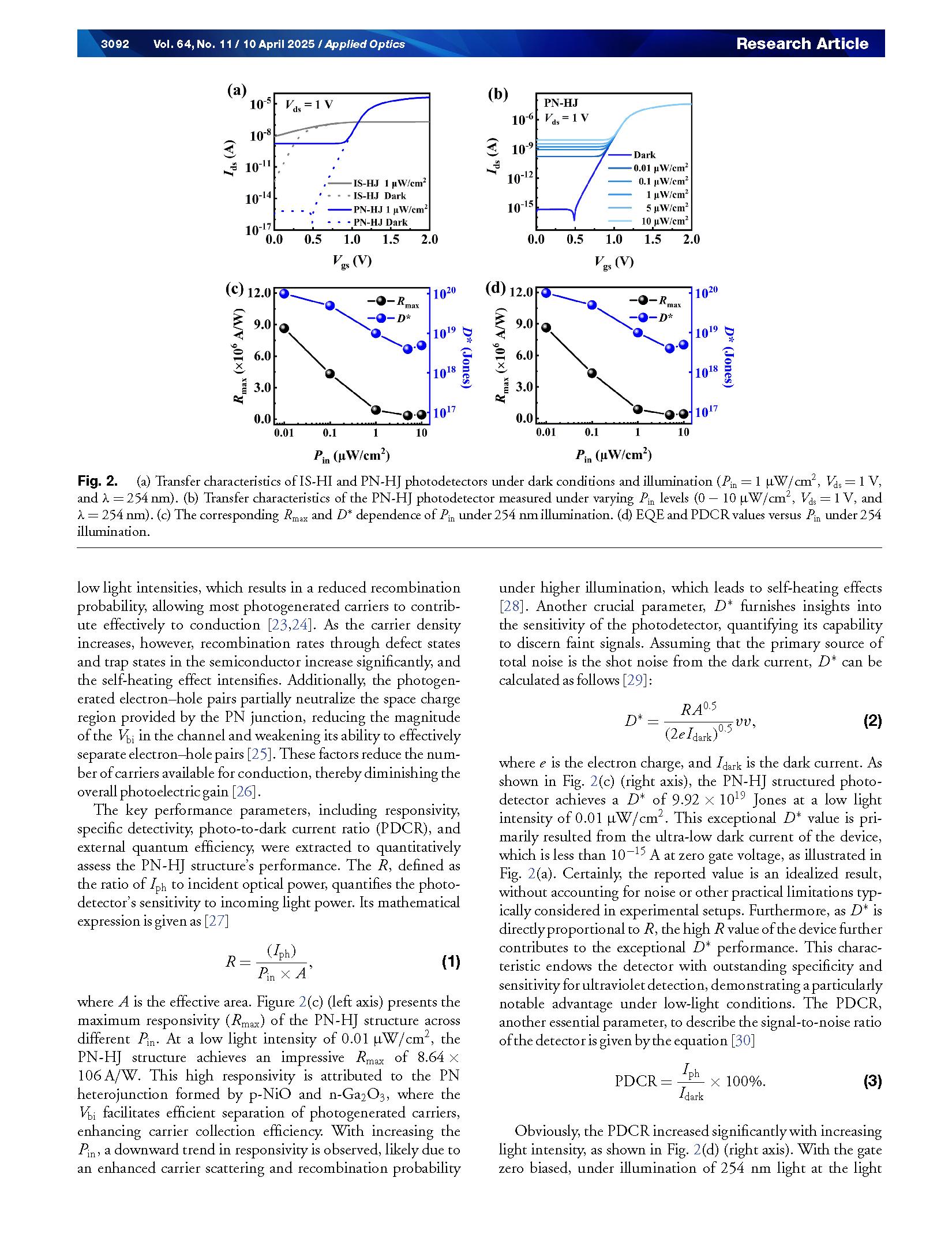
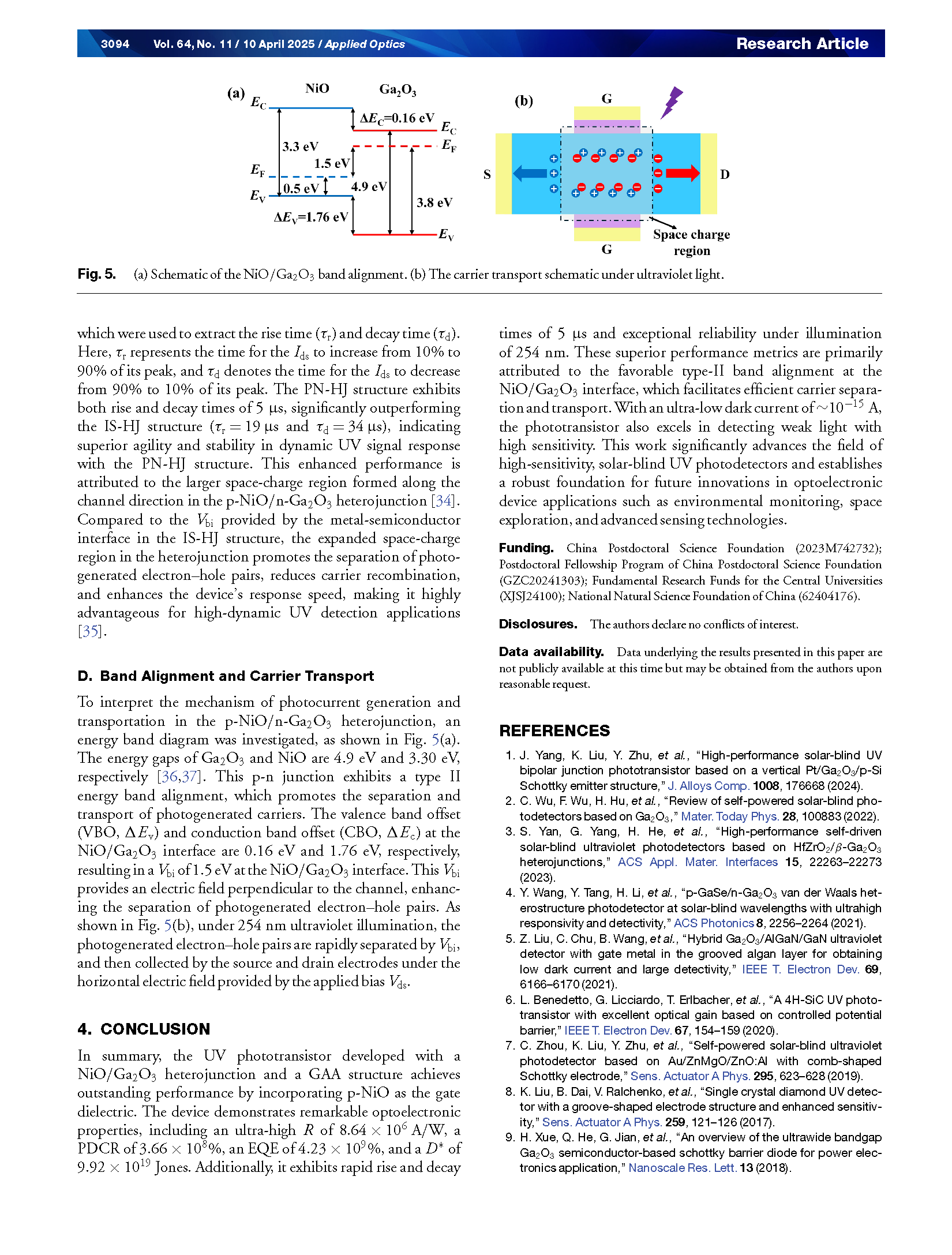
Gallium oxide (Ga2O3), with its ultra-wide bandgap of 4.9 eV, excellent thermal stability, and availability in large native substrates, is an ideal material for solar-blind ultraviolet (UV) detection. In this study, we present a high-performance gate-all-around (GAA) phototransistor based on a p-NiO/n-Ga2O3 heterojunction, specifically designed for advanced UV detection applications. The incorporation of p-NiO as the gate material provides a strong built-in electric field, which significantly improves carrier separation, suppresses dark current, and enhances the overall photoresponse. The constructed GAA phototransistor exhibits superior optoelectronic properties, including a responsivity of 8.64×10⁶A/W, an external quantum efficiency of 4.23×10⁹%, a detectivity of 9.92×10¹⁹ Jones, and rise/fall times both of 5 µs. Comprehensive simulation and experimental analyses reveal that the enhanced performance stems from the favorable type-II band alignment at the NiO/Ga2O3 interface, which facilitates efficient photocarrier generation and transport. This work not only establishes a pathway for developing high-sensitivity and fast-response UV photodetectors but also lays the foundation for further advancements in solar-blind optoelectronics for environmental monitoring, space exploration, and other critical applications.
Conclusion
In summary, the UV phototransistor developed with a NiO/Ga2O3 heterojunction and a GAA structure achieves outstanding performance by incorporating p-NiO as the gate dielectric. The device demonstrates remarkable optoelectronic properties, including an ultra-high R of 8.64 × 10⁶ A/W, a PDCR of 3.66 × 10⁸%, an EQE of 4.23 × 10⁹%, and a D∗ of 9.92 × 10¹⁹ Jones. Additionally, it exhibits rapid rise and decay times of 5 µs and exceptional reliability under illumination of 254 nm. These superior performance metrics are primarily attributed to the favorable type-II band alignment at the NiO/Ga2O3 interface, which facilitates efficient carrier separation and transport. With an ultra-low dark current of∼10−15 A, the phototransistor also excels in detecting weak light with high sensitivity. This work significantly advances the field of high-sensitivity, solar-blind UV photodetectors and establishes a robust foundation for future innovations in optoelectronic device applications such as environmental monitoring, space exploration, and advanced sensing technologies.
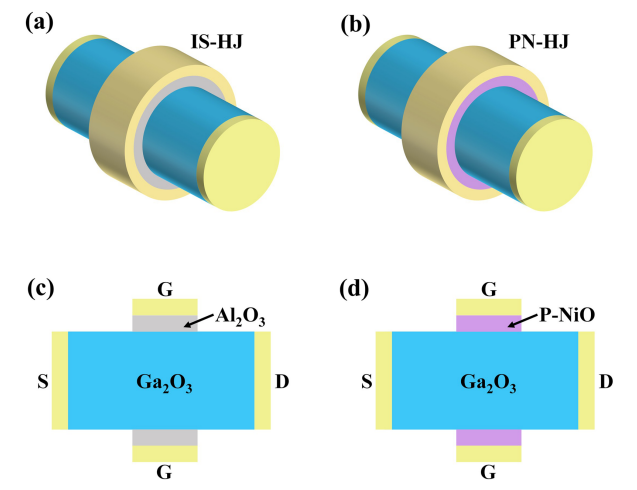
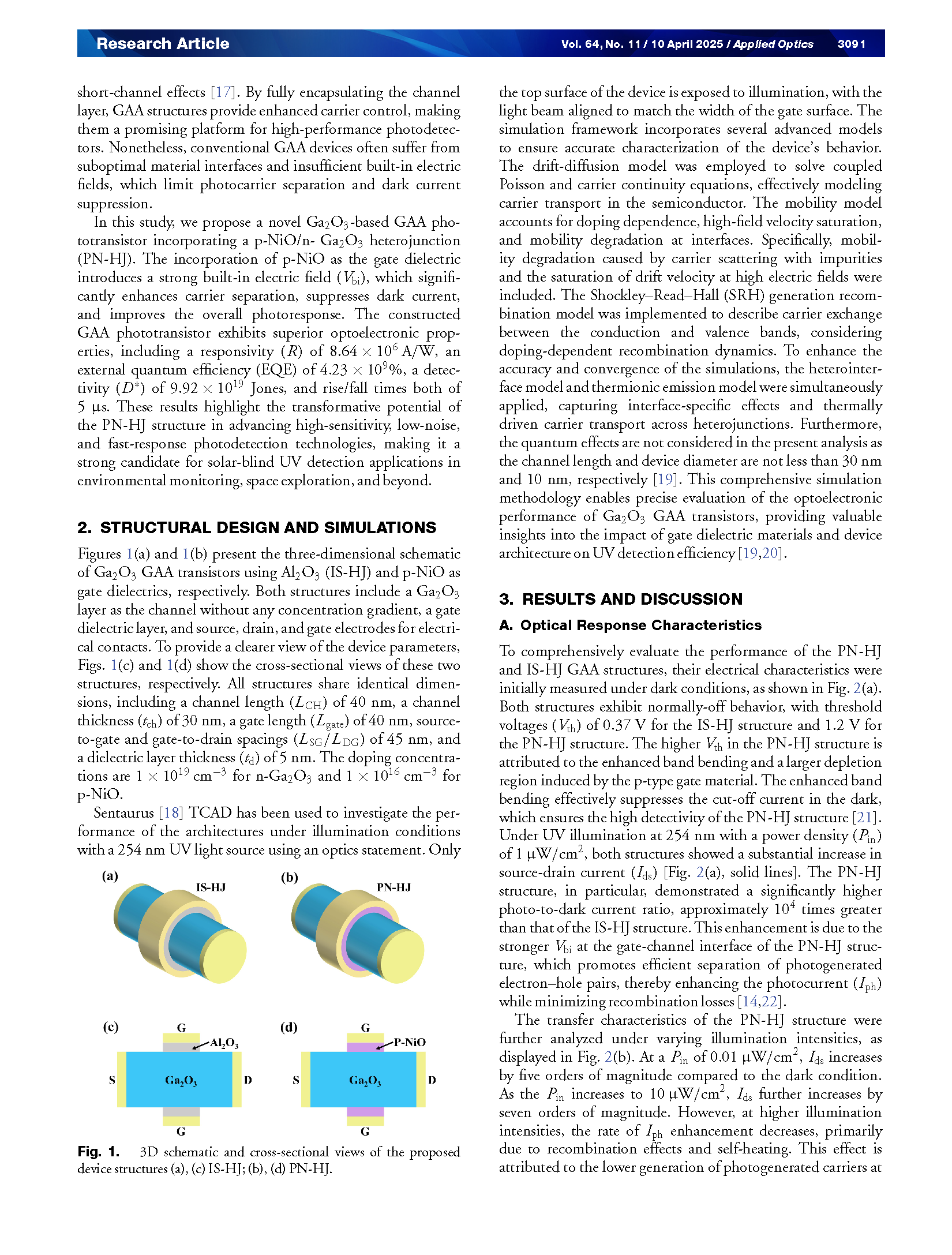
Fig. 1. 3D schematic and cross-sectional views of the proposed device structures (a), (c) IS-HJ; (b), (d) PN-HJ.
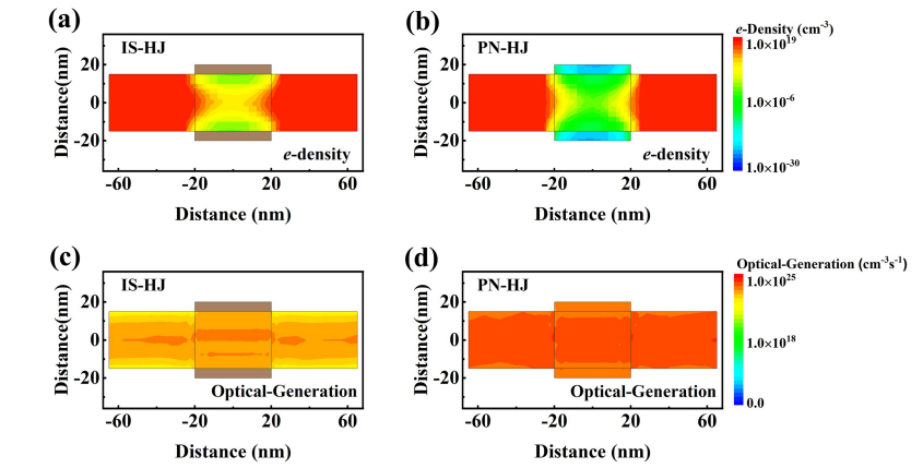
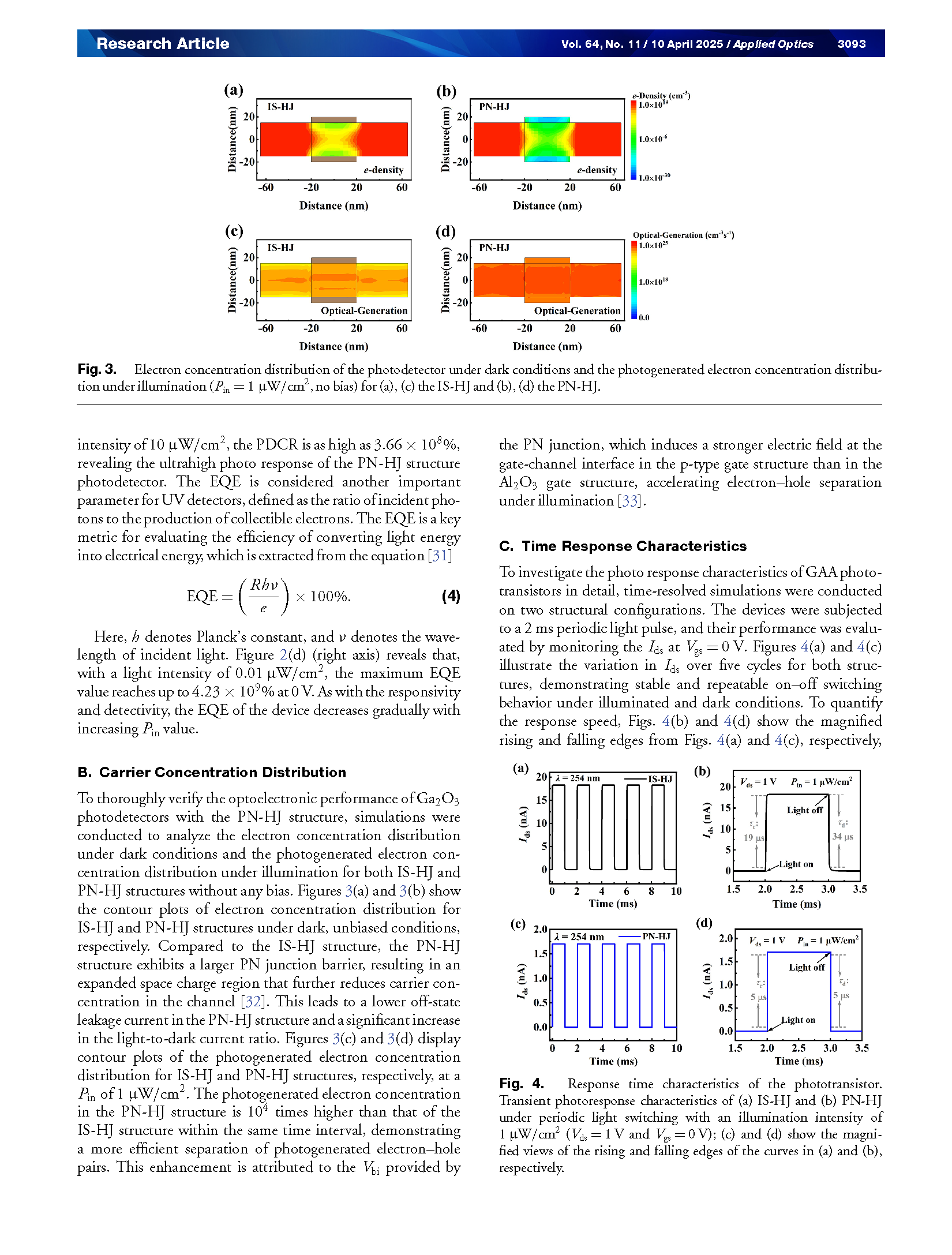
Fig. 2. Electron concentration distribution of the photodetector under dark conditions and the photogenerated electron concentration distribution under illumination (Pin = 1 µW/cm 2, no bias) for (a), (c) the IS-HJ and (b), (d) the PN-HJ.
DOI:
doi.org/10.1364/AO.551210