Paper Sharing
【International Papers】Gallium Oxide–Metal Interfaces: Insights from Density Functional Theory and Photodetection Performance Evaluation
日期:2025-04-23阅读:659
Researchers from the Hanoi University of Science and Technology have published a dissertation titled "Gallium Oxide–Metal Interfaces: Insights from Density Functional Theory and Photodetection Performance Evaluation" in Materials Research Express.
Background
Gallium oxide (Ga2O3) is a fourth-generation wide band gap semiconductor that has garnered significant attention due to its excellent properties and broad potential applications in power and optoelectronic devices. Among its five crystalline phases-α, β, γ, δ, and ε, the β-phase is the thermodynamically stable structure with a band gap of approximately 4.9 eV and has been extensively studied for its high performance in power devices. On the other hand, the metastable α-phase, with a wider band gap of 5.3 eV, offers distinct advantages for deep-ultraviolet transparency and advanced electronic applications. Although less stable, the α-phase holds significant promise for use in Schottky devices and related semiconductor technologies, where its unique electronic and optical properties can be leveraged to achieve superior device performance.
Abstract
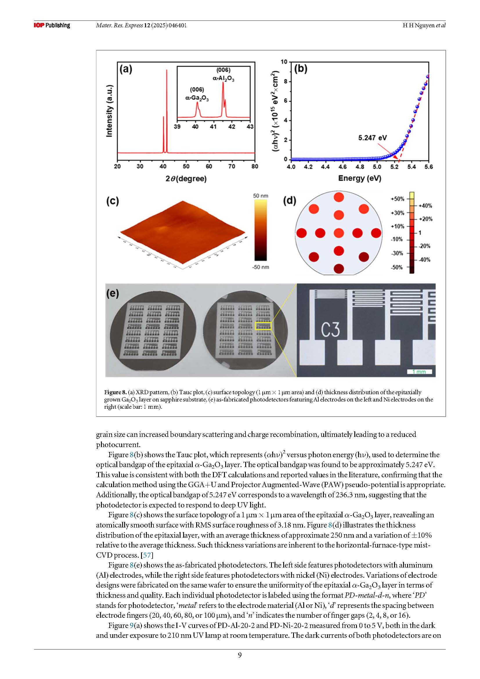
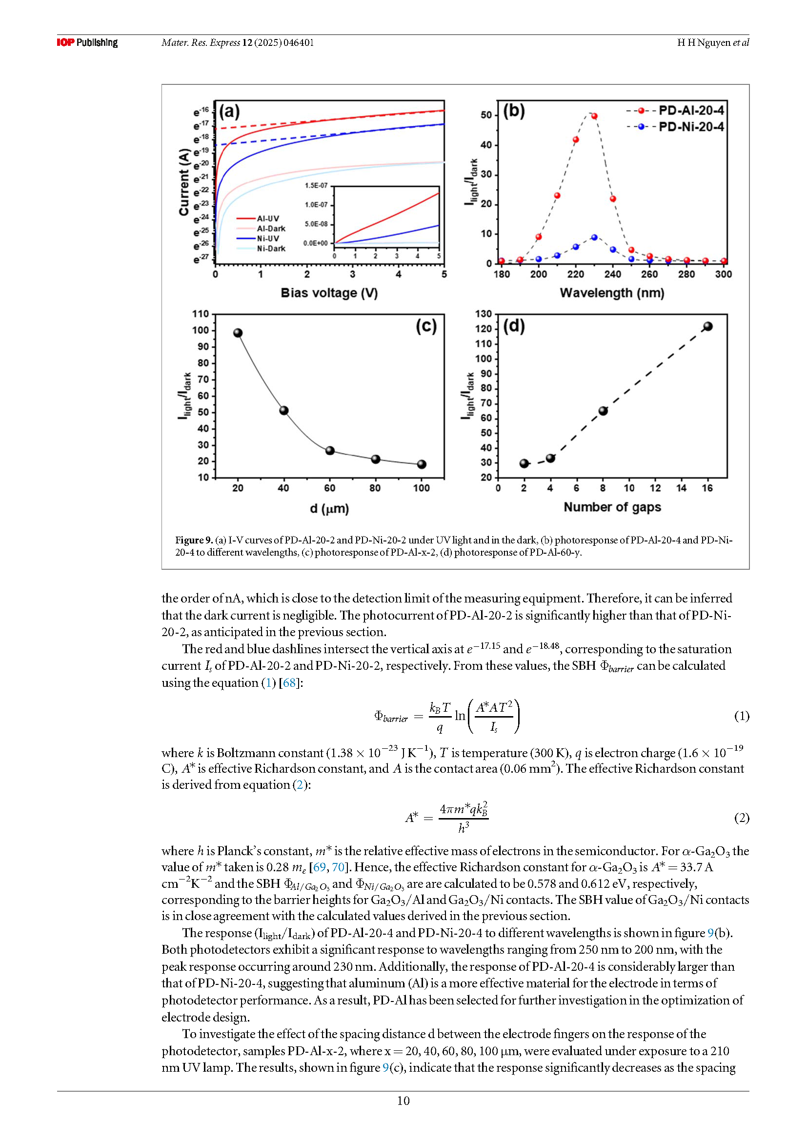
Gallium oxide (Ga2O3), a wide bandgap semiconductor of the fourth generation, shows great potential for advanced optoelectronic applications. While β-Ga2O3-based photodetectors (PDs) have been extensively studied, research on α-Ga2O3-based PDs remains scarce. This work investigates the structural, electronic, and performance characteristics of α-Ga2O3-based metal-semiconductor–metal (MSM) PDs. Using first-principles calculations within the GGA+U framework, it was found that Al(111) and Ni(111) electrodes interfacing with α-Ga2O3(0001) experience tensile and compressive strain, respectively. The bandgaps of bulk α-Ga2O3 were calculated as 5.30 eV (direct) and 5.17 eV (indirect), with negligible metal-induced gap states (MIGS) beyond the sixth Ga layer. The electron affinity of α-Ga2O3 is 4.31 eV, and the Schottky barrier heights for Ga2O3/Al and Ga2O3/Ni interfaces are 0.046 eV and 0.650 eV, respectively. Experimentally, symmetric MSM PDs were fabricated using mist-CVD for the epitaxial α-Ga2O3 layer and thermal evaporation for Al and Ni electrodes. The epitaxial layer demonstrated an optical bandgap of 5.247 eV. The PDs exhibited low dark current, with Al-electrode devices achieving a higher photo-to-dark current ratio compared to Ni-electrode devices. Peak photoresponse was observed around 230 nm, with smaller finger gaps and more electrode gaps enhancing performance. This study provides valuable insights into the interfacial properties and design optimization of α-Ga2O3-based PDs, demonstrating their potential for deep-ultraviolet optoelectronic applications.
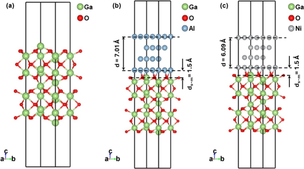
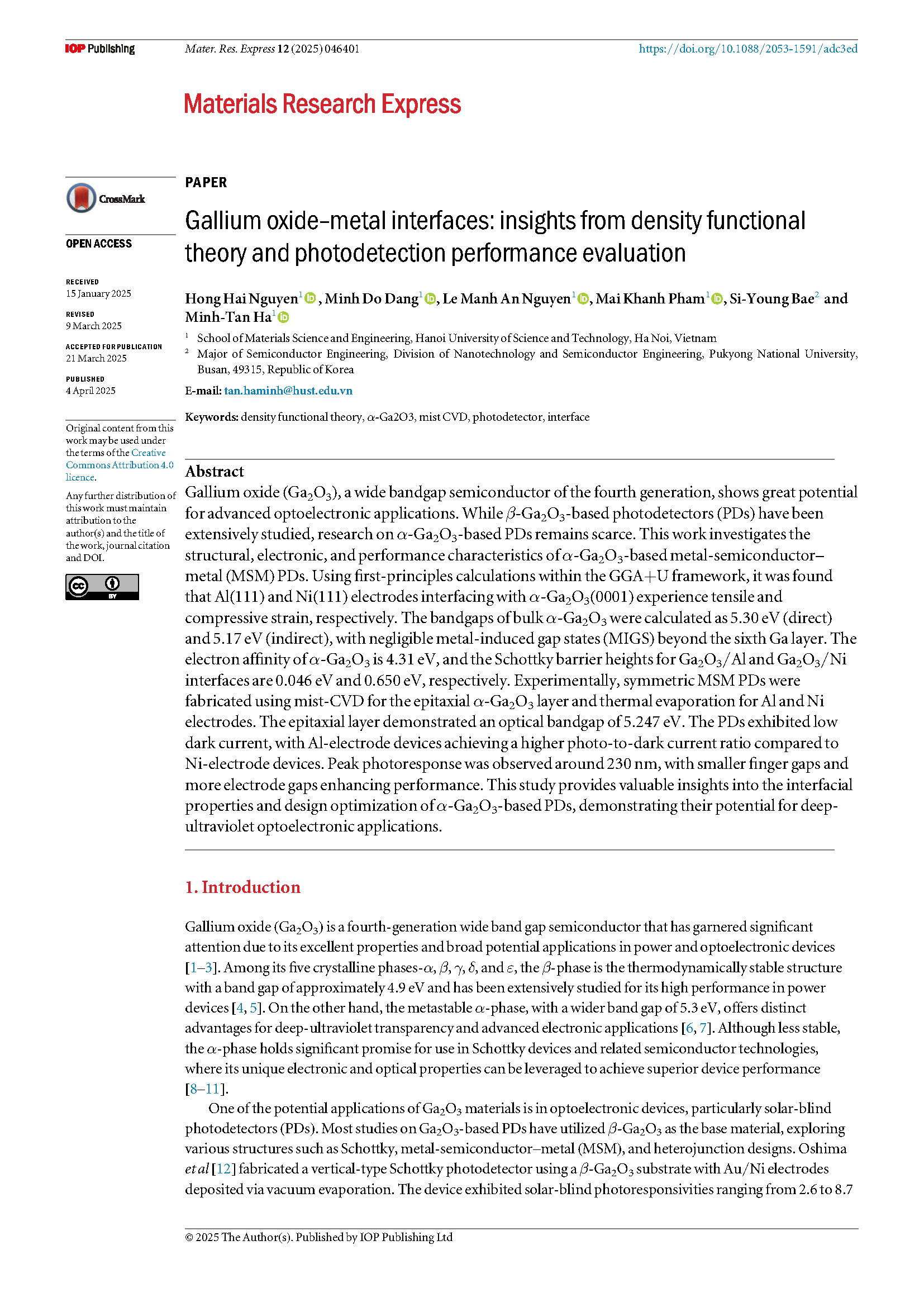
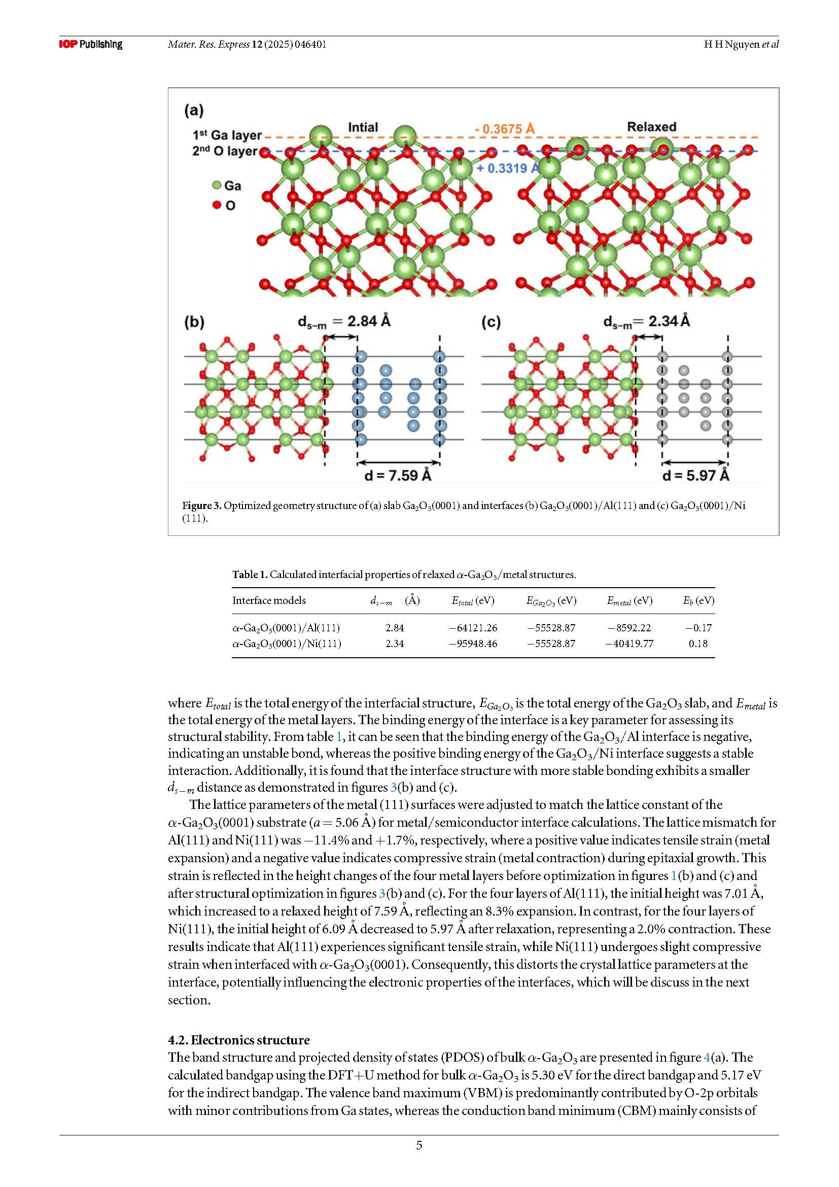
Figure 1. Intial modeling structure of (a) slab Ga2O3(0001) and interfaces (b) Ga2O3(0001)/Al(111) and (c) Ga2O3 (0001)/Ni(111).
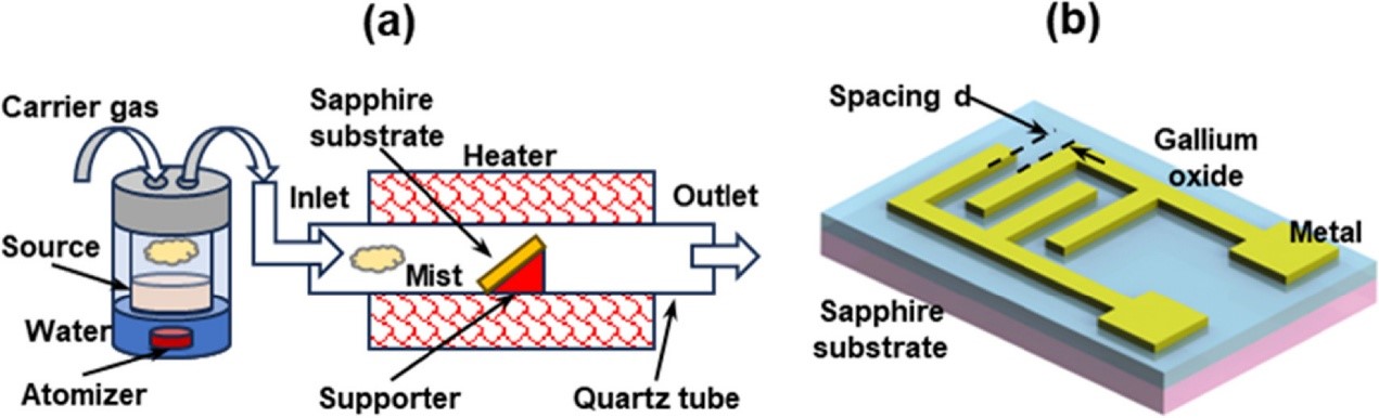
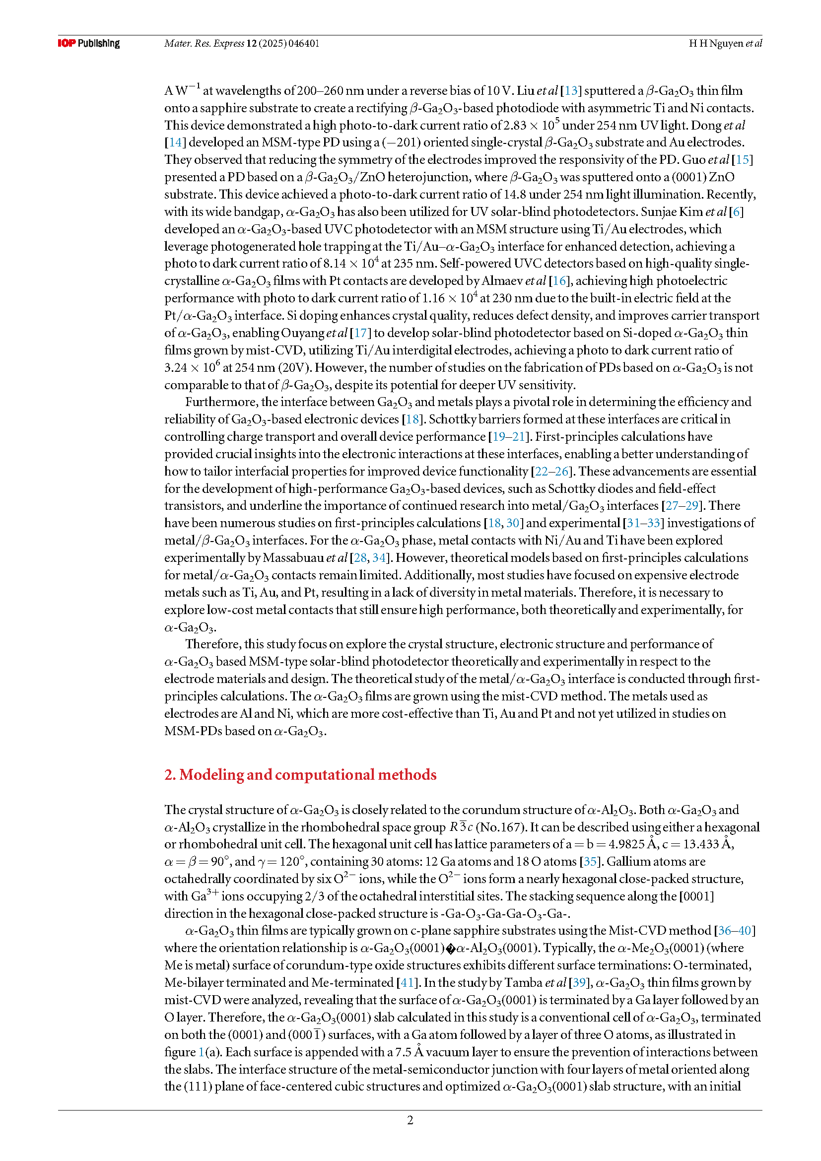
Figure 2. (a) Schematic of the mist-CVD system, (b) MSM structure of photodectors and electrodes designs.
DOI:
doi.org/10.1088/2053-1591/adc3ed