Paper Sharing
【Domestic Papers】Suppression of Hillock Defects on (010) β-Ga₂O₃ Homoepitaxial Layer Growth via Halide Vapor Phase Epitaxy
日期:2025-04-21阅读:688
Researchers from the Zhejiang University have published a dissertation titled "Suppression of Hillock Defects on (010) β-Ga2O3 Homoepitaxial Layer Growth via Halide Vapor Phase Epitaxy" in Crystal Growth & Design.
Project Support
This work was supported by the “Pioneer” and “Leading Goose” R&D Program of Zhejiang (2023C01193), the National Natural Science Foundation of China (52202150, 22205203, and 62204218), Fundamental Research Funds for the Central Universities (226-2022-00200 and 226-2022- 00250), the National Postdoctoral Program for Innovative Talents (BX20220264), the National Program for Support of Topnotch Young Professionals, and the Leading Innovative and Entrepreneur Team Introduction Program of Hangzhou (TD2022012).
Background
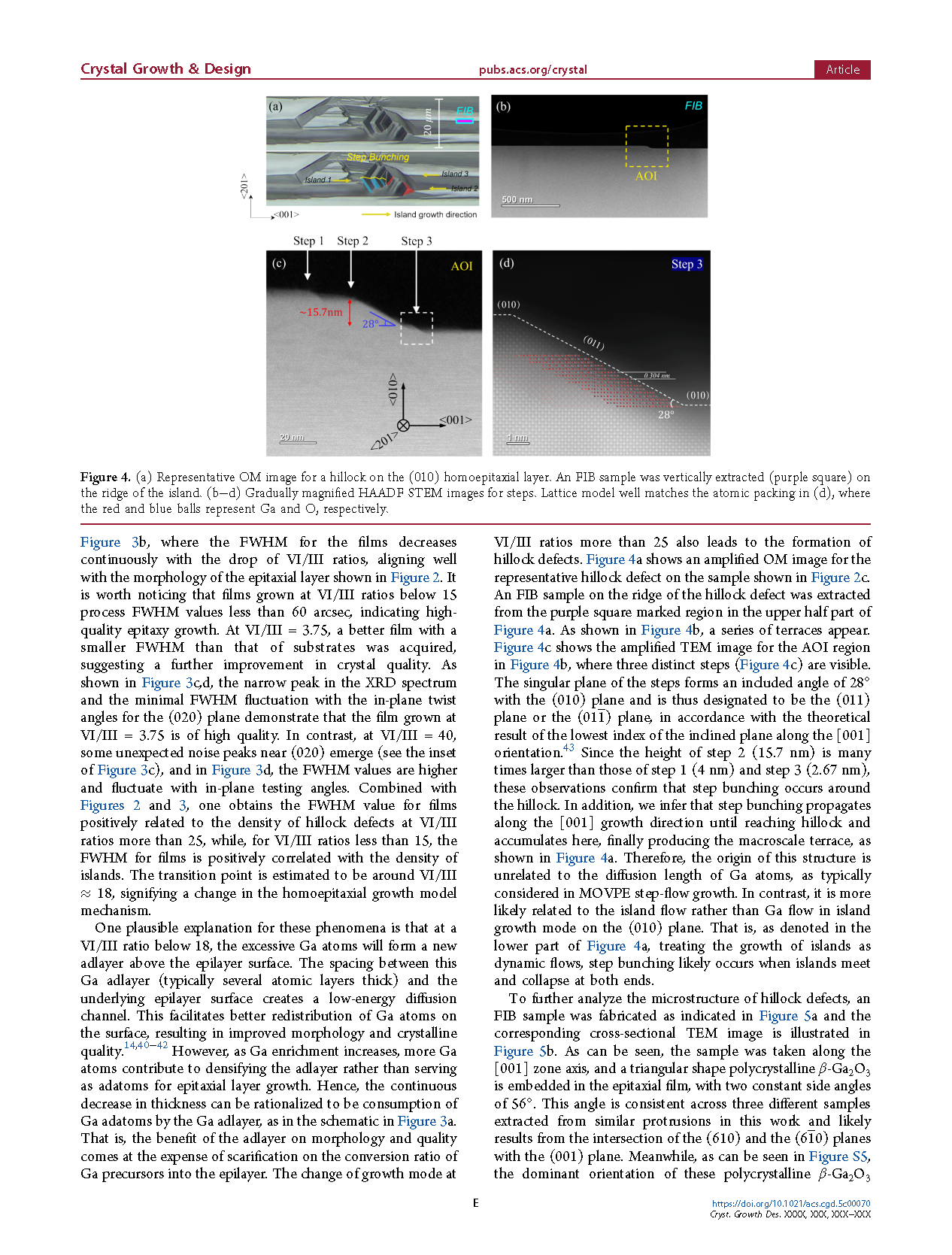
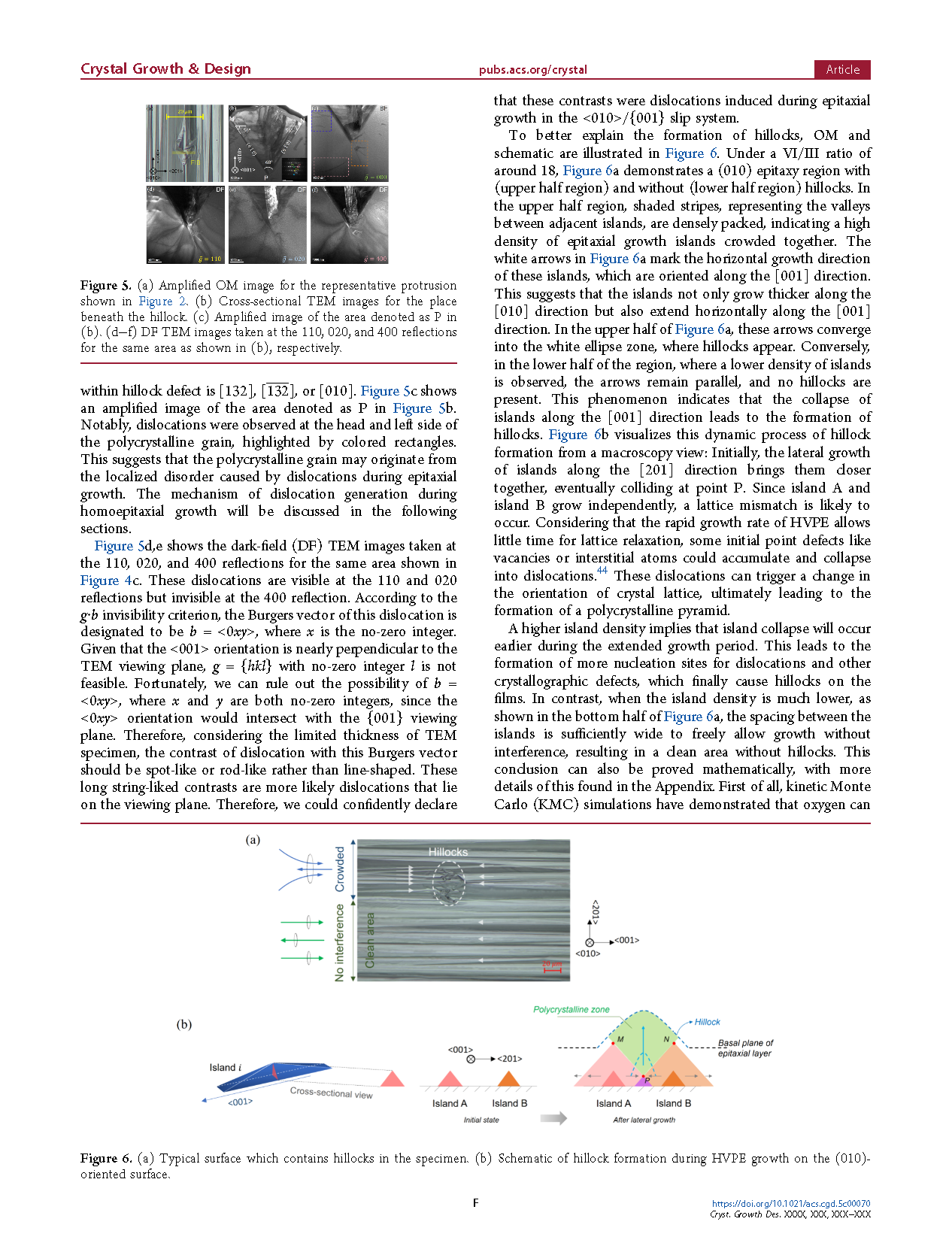
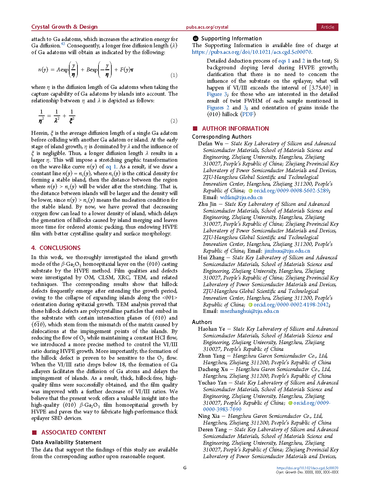
In this paper, it is the first time to use the casting growth β-Ga2O3 substrate for homoepitaxial growth. A high-quality, hillock-free, unintentionally doped (010) HVPE layer, with a thickness of 4−12 μm, was successfully grown on Sn-doped β-Ga2O3 substrates. The (010) HVPE films were thoroughly investigated via OM, CLSM, XRC, TEM, and related techniques. Our findings support the growth of the β-Ga2O3 layer on the (010) plane in the island growth mode. Meanwhile, a novel type of hillock frequently occurs on the films, which can be ultimately excluded via harnessing VI/III ratios less than 18 by decreasing the level of the O2 precursor flow while fixing the HCl flow. The nature of hillocks is unveiled by TEM examination, and the underlying mechanism on how O2 flow influences hillock formation is reasonably explained by the formation of the Ga adlayer and the modified Bales diffusion model. We believe this study could facilitate the fabrication of hillock-free (010) β-Ga2O3 homoepitaxial layers with enhanced conductivity, ultimately benefiting device performance.
Abstract
Hillock, a type of surface defect with small mounds or protrusion morphologies, can significantly impair the flatness and uniformity of β phase gallium oxide (β-Ga2O3) epitaxy, particularly on the (010) plane. Herein, a high-quality, hillock-free (010) β-Ga2O3 homogeneous layer with a thickness of ∼10 μm was successfully grown by halide vapor phase epitaxy (HVPE). The growth mode and hillock structure were thoroughly investigated via optical microscopy (OM), confocal laser scanning microscopy (CLSM), X-ray rocking curve (XRC) analysis, and transmission electron microscopy (TEM). The results indicate that these hillocks are polycrystalline particles, which generate along the <001> direction with specific intersection planes of (610) and (61̅0). By adjusting the flow of O2 while fixing the flow of HCl, a precise hillock hindrance method was implemented, resulting in a smoother (010) epitaxy surface at VI/III ratios below 18. This work offers a new perspective on the origin and suppression method of the hillock defect on HVPE (010) β-Ga2O3 layers, paving the path to fabricate high-performance power devices.
CONCLUSIONS
In this work, we thoroughly investigated the island growth mode of the β-Ga2O3 homoepitaxial layer on the (010) casting substrate by the HVPE method. Film qualities and defects were investigated by OM, CLSM, XRC, TEM, and related techniques. The corresponding results show that hillock defects frequently emerge after extending the growth period, owing to the collapse of expanding islands along the <001> orientation during epitaxial growth. TEM analysis proved that these hillock defects are polycrystalline particles that embed in the substrate with certain intersection planes of (610) and (61̅0), which stem from the mismatch of the matrix caused by dislocations at the impingement points of the islands. By reducing the flow of O2 while maintaining a constant HCl flow, we introduced a more precise method to control the VI/III ratio during HVPE growth. More importantly, the formation of the hillock defect is proven to be sensitive to the O2 flow. When the VI/III ratio drops below 18, the formation of Ga adlayers facilitates the diffusion of Ga atoms and delays the impingement of islands. As a result, thick, hillock-free, highquality films were successfully obtained, and the film quality was improved with a further decrease of VI/III ratios. We believe that the present work offers a valuable insight into the high-quality (010) β-Ga2O3 film homoepitaxial growth by HVPE and paves the way to fabricate high-performance thick epilayer SBD devices.
Graphic Examples
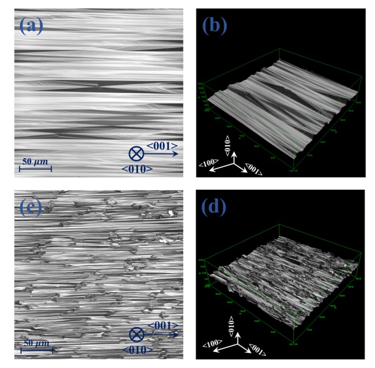
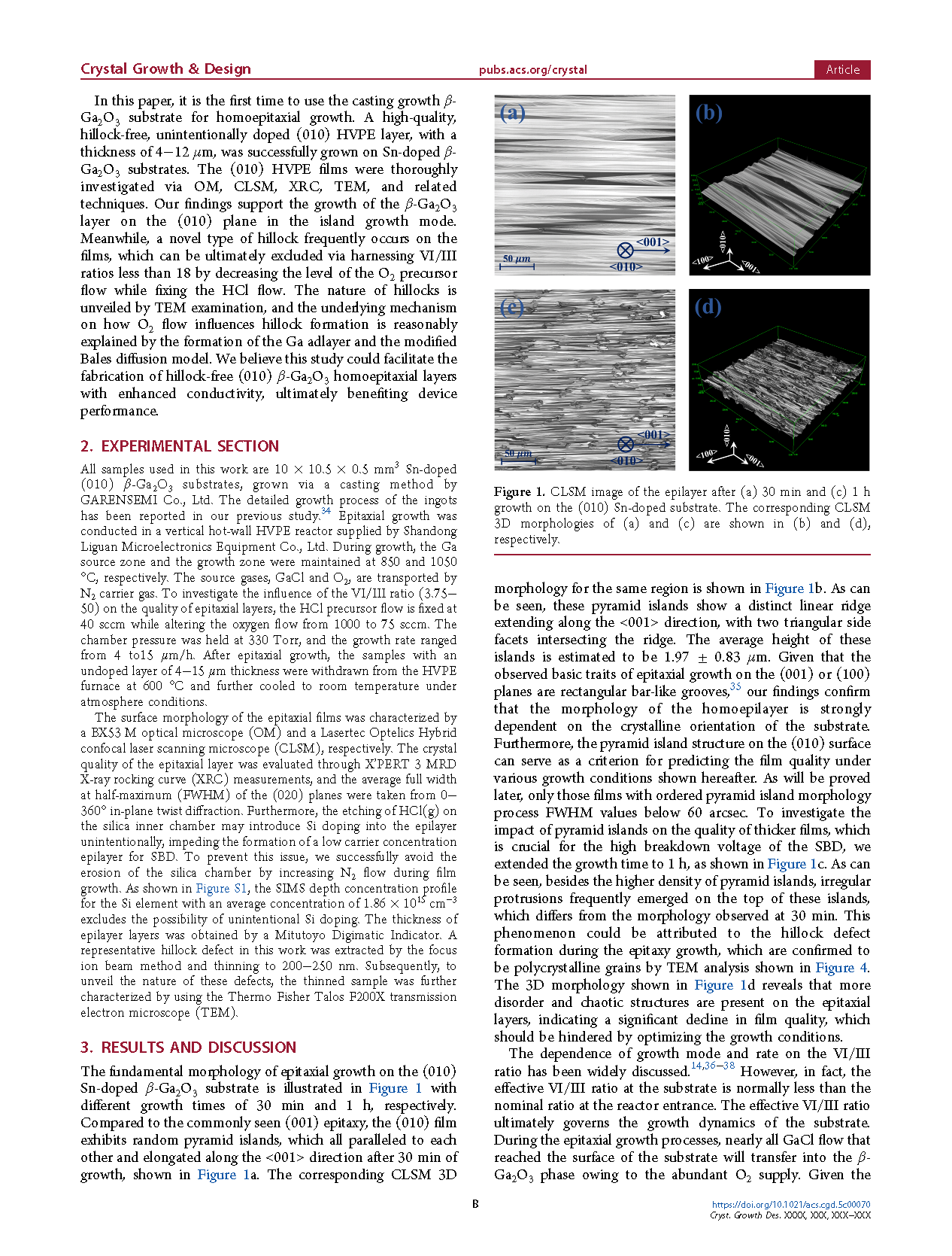
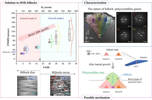
Figure 1. CLSM image of the epilayer after (a) 30 min and (c) 1 h growth on the (010) Sn-doped substrate. The corresponding CLSM 3D morphologies of (a) and (c) are shown in (b) and (d), respectively.
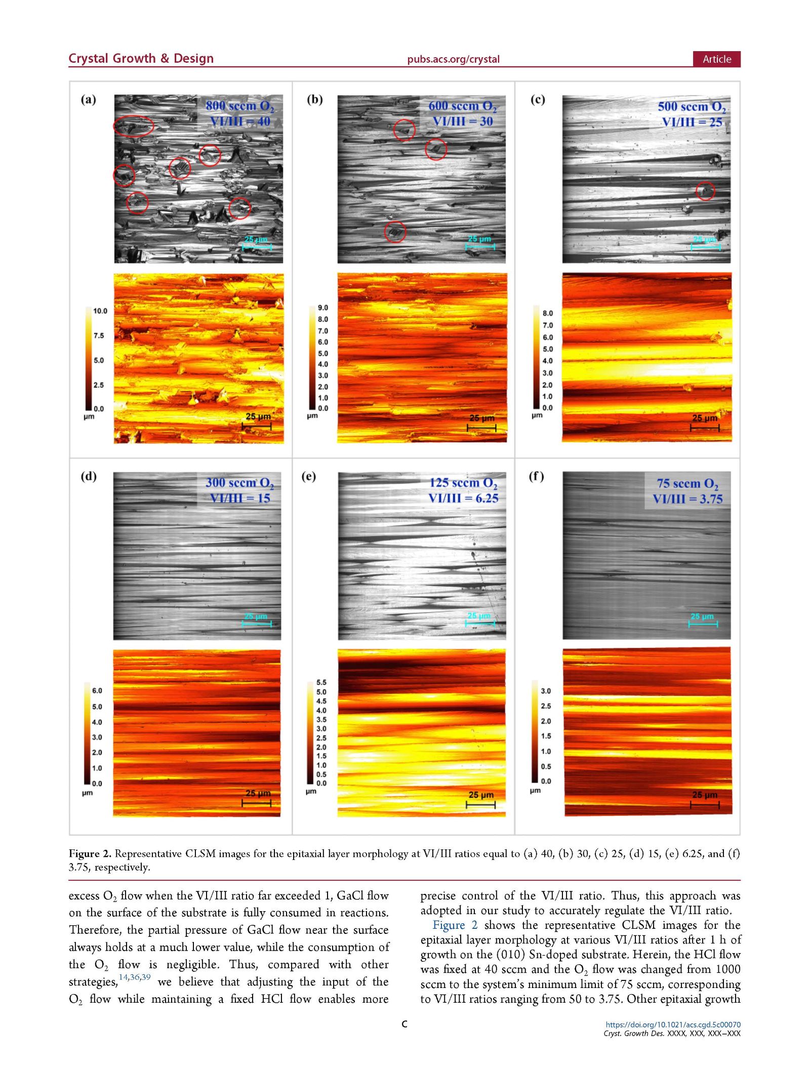
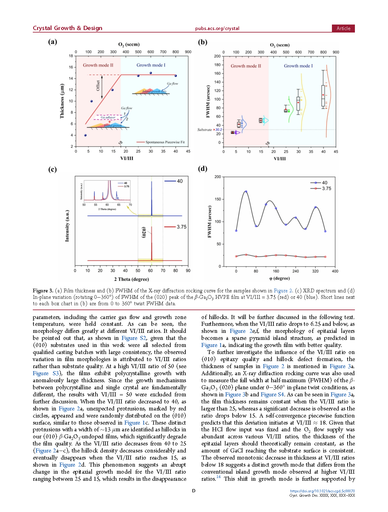
Figure 2. Representative CLSM images for the epitaxial layer morphology at VI/III ratios equal to (a) 40, (b) 30, (c) 25, (d) 15, (e) 6.25, and (f) 3.75, respectively.
DOI:
doi.org/10.1021/acs.cgd.5c00070