


Member News
【Member News】JFS Lab Launches Research-Grade Ga₂O₃ Power Discrete Devices & "Coupon-to-Wafer" Tape-Out Platform
日期:2025-04-18阅读:881
Recently, the Jiufengshan Laboratory (JFS Lab) has provided the "Coupon to wafer" wafer fabrication research and development platform for Gallium Oxide to various scientific research institutions, and at the same time offers a variety of research-grade power device packaging single tubes. Including JFS's innovative Planar SBD, Trench SBD (Schottky Barrier Diode) devices and planar MOSFET devices. They are all manufactured based on all-Gallium Oxide materials, marking that JFS Lab has achieved a relatively good technical accumulation in the R&D process platform of Gallium Oxide semiconductor devices. The SBD and MOSFET research-grade packaged devices released this time are designed to meet customers' demands for testing, analysis and application exploration of Gallium Oxide devices, and further promote the industrialization development of the Gallium Oxide industry.
00 JFS Ga2O3 "Coupon to Wafer" Technology Tape-Out Platform
JFS Ga2O3's "coupon to wafer" technology enables the development and small- lot production of small-sized WBG materials on 6/8-inch mass production fab line. This allows small-sized materials to also be mass-produced using 6/8-inch high-precision stable process equipment. Meanwhile, future implementations could achieve heterogeneous integration of WBG devices with silicon CMOS logic control, expanding multi-material and multi-functional integration technology, and simultaneously enhancing the heat dissipation capacity of Gallium Oxide devices.

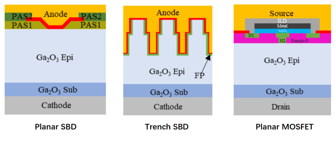
01 Planar SBD
Product Highlights and Features
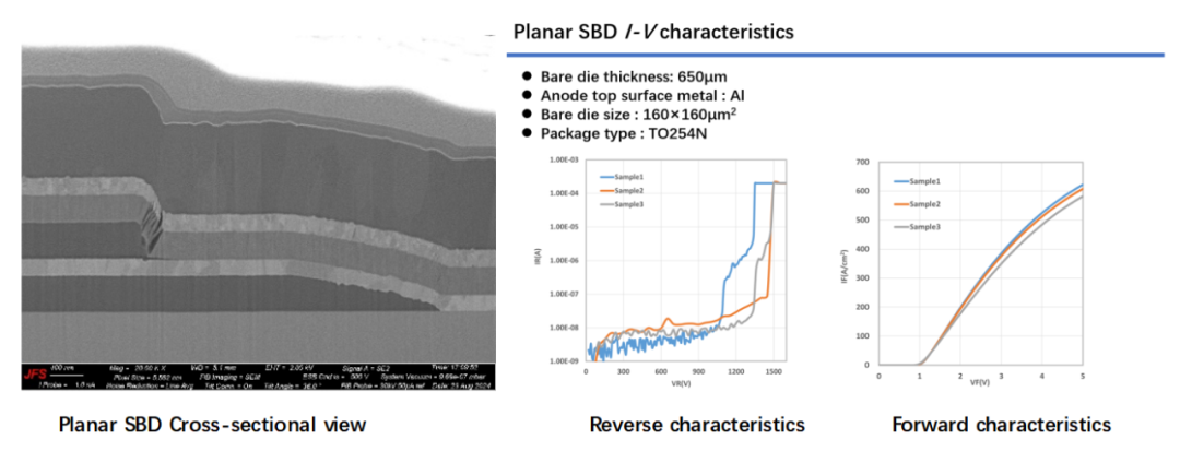
The Planar SBD device launched by JFS Lab this time is simple to manufacture, has a large forward current density and high reverse voltage, and is specially designed for studying the electrical properties of Gallium Oxide devices and early application exploration.
·Specifications: Electrode sizes are available in various specifications such as 110*110 (μm2), 2*2(mm2), and customizable requirements bare die and package forms are available for customers, suitable for specific test and application scenarios.
02 Trench SBD
Product Highlights and Features
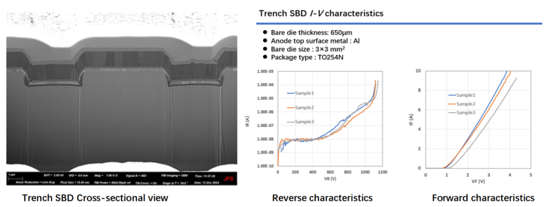
JFS Lab features a unique IP two-level trench SBD structure, which provides better Schottky region masking, enhances reliability while maintaining a good current path and forward conduction capability. Core patents include CN113990801A, CN119486231A, CN116207164A, etc.
·Specification: The electrode size is 2.5*2.5 (mm2), and bare die and package forms of the device are available for customers, suitable for specific test and application scenarios.
03 Planar MOSFET
Product Highlights and Features
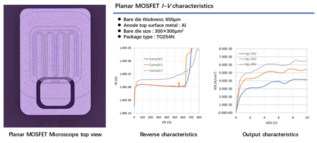
The first vertical MOSFET of JFS Lab that constructs a gate electric field shielding structure by forming a high-resistance region through nitrogen injection has highly reliable gate electric field protection in future practical applications (the critical electric field in Gallium Oxide can theoretically reach 8MV/cm, which is much higher than 3MV/cm of SiC), and it has unique IP series intellectual property rights. Core patent CN116705616A.
·Specification: Test sample (4 cells only) electrode size 250*250 (μm2), high current specification chips (5-20A) will be gradually introduced later, bare die and package form devices available for customers, suitable for specific test and application scenarios.
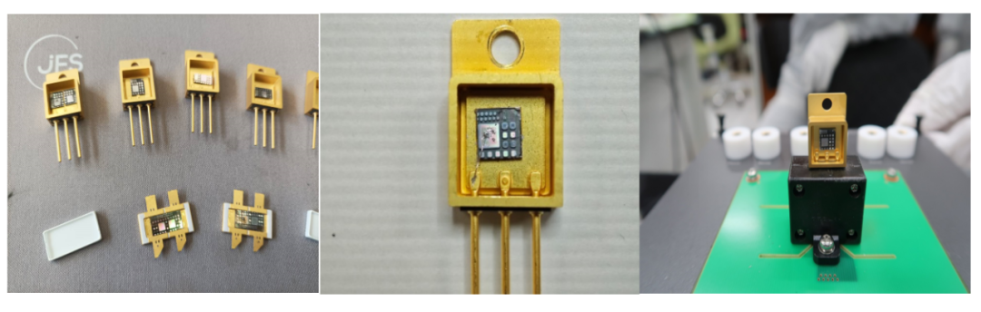
04 Device Package
Packaging Form: TO Metal Packaging
For inquiries and purchase, please contact wangkuan@jfslab.com.cn
