Conference News
【Conference News】Alliance Meets You at 2025 Semiconductor New Materials Development (Wuxi) Conference — Highlights of Gallium Oxide Preview
日期:2025-04-15阅读:1435
The Semiconductor Materials Branch of China Electronic Materials Industry Association is scheduled to hold the "2025 Semiconductor New Materials Development (Wuxi) Conference" in Wuxi, Jiangsu Province from April 16 to 19, 2025. This conference focuses on the new challenges of the global semiconductor industry under the new situation, the new situation, the new technology and the new demand generated by the market, with the theme of "New Situation, New Materials and New Challenges", and focuses on the development and device application of new semiconductor materials such as silicon carbide, Gallium Nitride, Gallium Oxide, Aluminum Nitride and Diamond.
For the highlights of Gallium Oxide in this conference, we will browse for you one by one, and the whole is divided into three parts: Member Exhibitors, Expert Reports, Alliance Activities.
Member Exhibitor※ The ranking is in the order of booth number
Shandong Liguan Microelectronics Equipment Co.,Ltd
Booth number: 17
Shandong Liguan Microelectronics Equipment Co., LTD. (abbreviation: Shandong Liguan), founded in 2013. After 12 years of development, Shandong Liguan has become a domestic and foreign advanced semiconductor equipment manufacturing and process technology service provider integrating R&D, production and sales.
The company's products cover the first generation to the fourth generation of semiconductor material process equipment, all with independent intellectual property rights, completely independent and controllable, products are widely used in integrated circuits, power semiconductors, compound semiconductors, 5G chips, optical communication, MEMS and other new electronic device manufacturing fields.
The company can provide customers with an integrated solution of "equipment manufacturing + process technical service".
The company always firmly believes in the scientific development concept of "scientific and technological innovation is the first productive force", adheres to innovation-driven, innovation-led, and deeply cultivates the semiconductor industry. Committed to promoting the development of semiconductor material manufacturing and equipment technology, through continuous innovation and investment, constantly break through the technical bottleneck, improve product performance and quality, meet market demand, achieve localization substitution, promote the high-quality development of China's semiconductor industry, and contribute to the development of China's semiconductor industry.
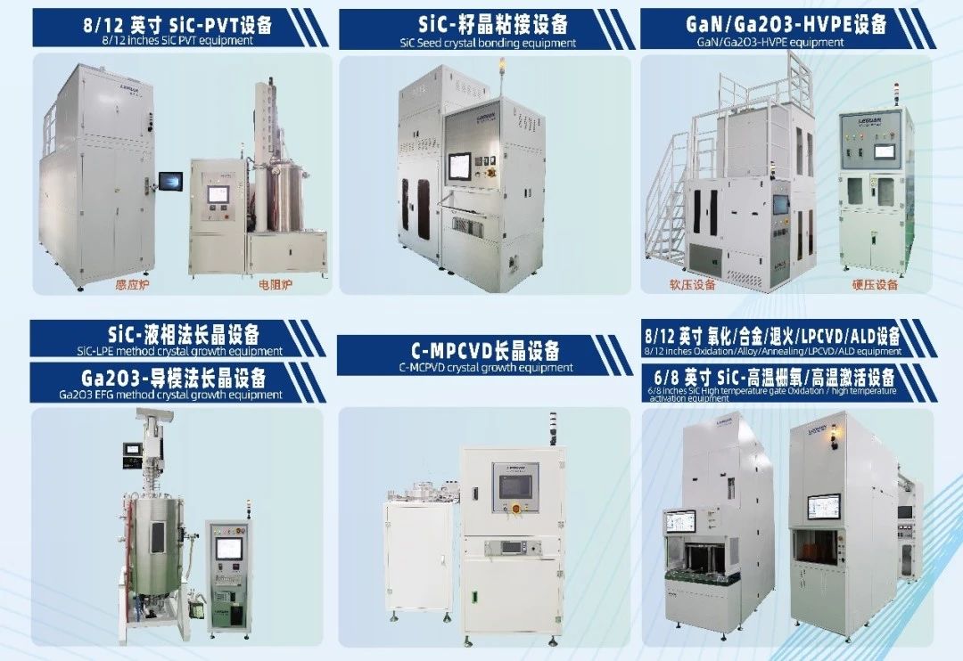
Main products
I.Semiconductor process equipment:
1, Oxidation/diffusion/annealing equipment
Vertical furnace, horizontal furnace, SiC high temperature oxidation furnace, SiC high temperature annealing furnace
2, CVD equipment
LPCVD vertical furnace, LPCVD horizontal furnace
II. Compound crystal equipment:
1, SiC single crystal growth equipment
PVT furnace (induction furnace, resistance furnace), liquid phase crystal growth furnace, seed crystal bonding equipment (soft pressing equipment, hard pressing equipment)
2, GaN single crystal growth equipment
HVPE crystal growth furnace (horizontal, vertical)
3, Ga2O3 single crystal growth and epitaxy equipment
EFG crystal growth furnace, Vertical Bridgman method (VB) furnace (non-iridium technology), HVPE epitaxial furnace (horizontal, vertical)
4, diamond single crystal growth equipment
MPCVD crystal growth furnace
5, GaAs/InP single crystal growth equipment
Crucible lowering furnace
Hangzhou GAREN Semiconductor Co., LTD
Booth number: 42
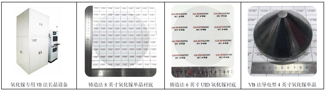
Hangzhou GAREN Semiconductor released the world's first 8-inch Gallium Oxide single crystal on March 5, 2025. GAREN SEMI is a technology enterprise focusing on the research and development, production and sales of wide band gap semiconductor materials such as Gallium Oxide. Relying on the National Key Laboratory of Silicon and Advanced Semiconductor Materials of Hangzhou International Science and Technology Innovation Center of Zhejiang University, the company has built a research and development, production and operation team with academicians of Chinese Academy of Sciences as the chief consultant and rich industry experience. The company created a new technology for Gallium Oxide single crystal growth, and obtained 14 international and domestic invention patents, breaking the monopoly and blockade of Western countries on Gallium Oxide substrate materials. Based on solving the major national needs, GAREN SEMI will be deeply engaged in the continuous innovation of the Gallium Oxide upstream industry chain, and strive to provide product guarantee for the development of China's power electronics and other industries.
GAREN SEMI leads the industry in innovation, achieving technological breakthroughs in the production of 6-inch Gallium Oxide single crystal substrates and wafer-grade (010) single crystal substrates using self-developed single crystal growth technologies such as the casting process, and developing the first dedicated Gallium Oxide VB long-crystal equipment including process packages. The company has mastered the core technology of Gallium Oxide growth, processing, epitaxy and other whole chain, providing customers with large-scale high-quality Gallium Oxide products and equipment with complete independent intellectual property rights.
Core Product
Hangzhou Fujia Gallium Technology Co., LTD
Booth No. 50
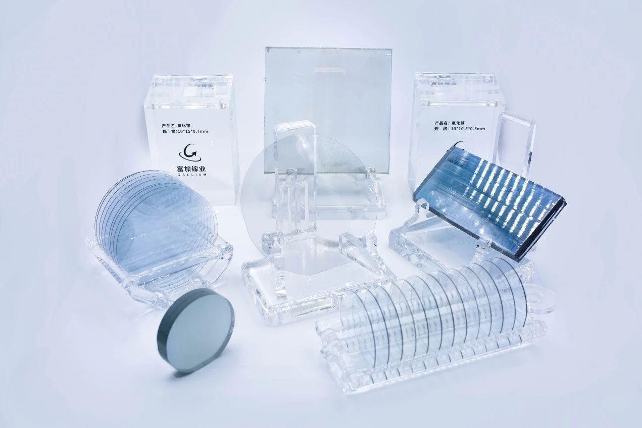
Hangzhou Fujia Gallium Technology Co., LTD., founded on December 31, 2019, is the first "hard technology" enterprise registered by Hangzhou Institute of Optics and Fine Mechanics. With the vision of "making the world use good materials", the company carries out the industrialization work of wide band gap semiconductor Gallium Oxide materials. The core products are Gallium Oxide single substrate, MOCVD epitaxial wafer, MBE epitaxial wafer, and Gallium Oxide crystal growth and processing equipment. The products mainly serve the fields of power devices, microwave radio frequency and photoelectric detection.
It has obtained 12 international patent licenses (6 in the United States and 6 in Japan), 40 domestic patent licenses, 3 trademark certification registrations of "Fujia Gallium" and 3 software Copyrights (" one-click crystal growth "control software).
Main products
·2/4/6 inch Gallium Oxide wafer
·Gallium Oxide epitaxial wafer (MBE)
·Gallium Oxide epitaxial wafer (MOCVD)
·Gallium Oxide crystal growth furnace
·Gallium Oxide wafer polishing machine
Expert Report
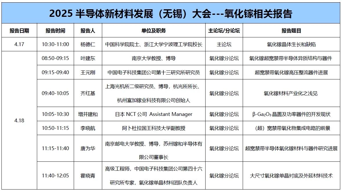
The relevant reports of Gallium Oxide in this conference have been sorted out in the table below, you are welcome to check.
Alliance Activity
The Asian Gallium Oxide Alliance participated in the exhibition as a partner of the organizer of this conference, aiming to introduce and promote the alliance to the participants and promote the development of the ultra-wide band gap semiconductor new materials industry. The alliance adheres to the concept of “Focused, Professional and Dedicated" to create a professional communication platform in the field of Gallium Oxide. During the conforence, alliance will organize lucky draw activities with good gifts, welcome new and old members to participate actively.
Alliance members continue to recruit, welcome everyone who has insight to create Gallium industry!
Booth number: 49