


Discover
【Knowledge Discover】Core Technology Affecting Semiconductor——Observation of Crystal from the Perspective of Symmetry (3)
日期:2025-04-14阅读:1353
Reading Guidance
Knowledge Discover is a new popular science column launched by the official account, focusing on in-depth analysis of cutting-edge materials and basic science. We will focus on the emerging semiconductor material of "Gallium Oxide", from crystal structure, physical properties to application scenarios, to comprehensively understand its breakthrough potential in fields such as 5G communication and new energy vehicles. At the same time, the column will also explore the scientific principles of Gallium Oxide materials and reveal their wide applications in energy, environmental protection, electronics and other fields.
Profile of Original Author
Hajime Okumura,Doctor of Engineering (Osaka University). Representative of Innovative Semiconductors, Electronics, & Energy Solutions, a limited liability partnership. Honorary Researcher of National Institute of Advanced Industrial Science and Technology. Honorary Associate Professor of University of Tsukuba.
In the previous article, the relationship between hexagonal and trigonal crystal systems is sorted out, and the problem of defects caused by symmetry differences is discussed with the hexagonal crystal based on HCP (hexagonal closest packing). Next, the differences between trigonal and hexagonal crystal systems will be discussed in detail, especially the characteristics of monoclinic crystal systems from the perspective of packing structure, and finally the series of articles will be summarized.
The Crystal System of the Stacking Structure
In the second half of the previous article, the crystal structures and defects formed by regular intra-layer displacement of layers with the closest packing structure are sorted out, and the Zhdanov meter is introduced as its representation. Regarding the stacking structure along the C-axis, here are some key points:
·The lattice that makes up the layers is a hexagonal net, and the atoms can be placed at three sites: lattice point A, site B with in-plane coordinates of (2/3, 1/3), and site C with in-plane coordinates of (1/3, 2/3).
·There are two kinds of structure of the layers: an α structure with symmetry of the layer group p 3m1, and a β structure obtained by rotating the axis that perpendicular to the layer of 180°. (Regarding names, you can name α and β any way you want, as long as you can distinguish between the two.)
·The lattice points of the nearest upper layer of a certain layer follow the order of "A → B → C → A →..." in the alpha structure compared to the lattice points of the nearest lower layer, while in the beta structure they follow the order of "A → C → B → A →...". Like this, it is only determined by the structure of the layers. This relationship can be well represented by the triangular prism diagram in Figure 3-1.
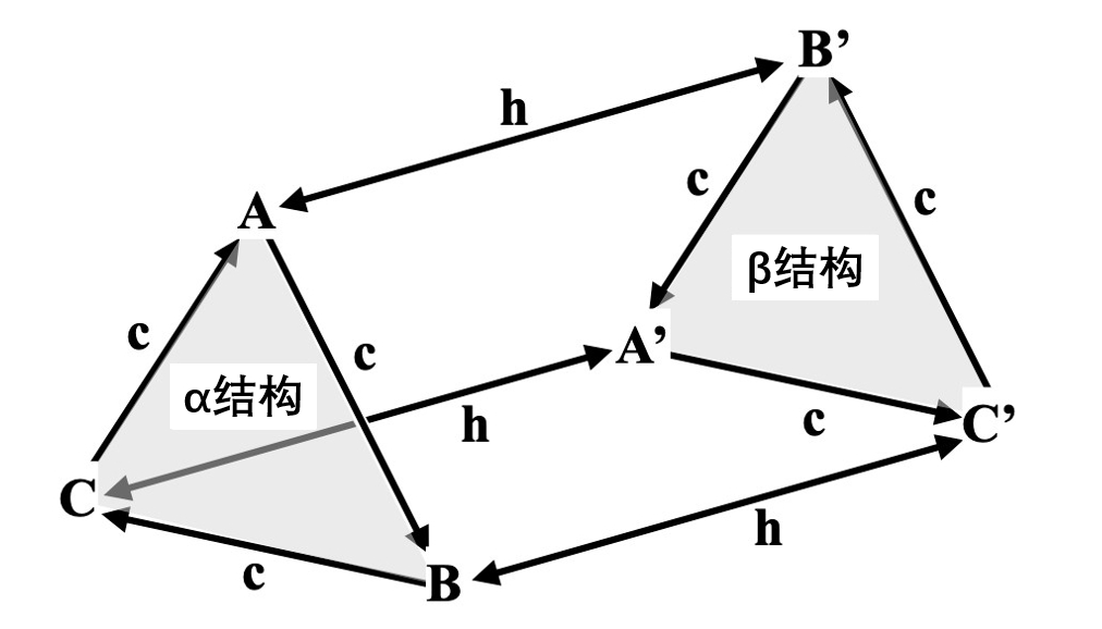
Figure 3-1. Relationship between sites and layer structure
For stacking structures using the Zhdanov method, in theory, using (m1 -n1 m2 -n2 … mr -nr) 0has translational symmetry, so it is possible to conceive crystals corresponding to its structure. So, what would be the crystal system of such a crystal?
Let's say the lattice point of layer 1 is at site A. Above it is built (m-1n1 m-2n2... m-rnr) stacked structure. According to the key points above, the lattice points of each layer are located at one of the A, B, or C sites. When the number of layers is L=Σ (mi+ni), if the lattice point of the L+1 layer is the same as that of the first layer (that is, the A site), then the original hexagonal lattice with the distance between the first layer and the L+1 layer is the length of the C-axis as the crystal system of the single cell, that is, the crystal of the hexagonal system. For example, the wurtzite type stacking structure is represented by (1-1), and at this time L=2, it is indeed an HCP structure taking two layers as the length of the C-axis. In the case of 6H-SiC, (3-3) represents L=6, again a hexagonal crystal with a period of 6 layers.
So what happens if the lattice point of layer L+1 is site B or site C? At first glance, a structure similar to the original monoclinic lattice may be formed, but in reality, repeating the structure of layers 1 through L three times will result in the rhombohedral structure shown in Figure 2-4. A typical example would be a 15R-SiC crystal (Zhdanov notation is (3-2)3=(3-2 3-2 3-2), L=15). In the next period after the represented fundamental period (3-2), the lattice point is at site B, the second period is at site C, and the third period returns to site A. The site corresponds to the layer structure as "ABCA 'c 'bcab 'A 'cabc 'b 'a". Figure 3-2 shows the stacking structure of 15R-SiC, which can be confirmed to be consistent with the above notation, and the 16th layer has the same site configuration as the 1st layer. Furthermore, after considering the three cycles, the original trigonal lattice as shown by the solid red line in Figure 3-2 can be set up. However, due to the influence of extremely long periods in the direction of the C-axis, a significantly elongated trigonal lattice with an Angle between the long fundamental translation vector and the small translation vector is formed. Back to the question, if the end point of the original periodic structure is the same, then it is hexagonal crystal system; If they are different, it is a trigonal crystal system.
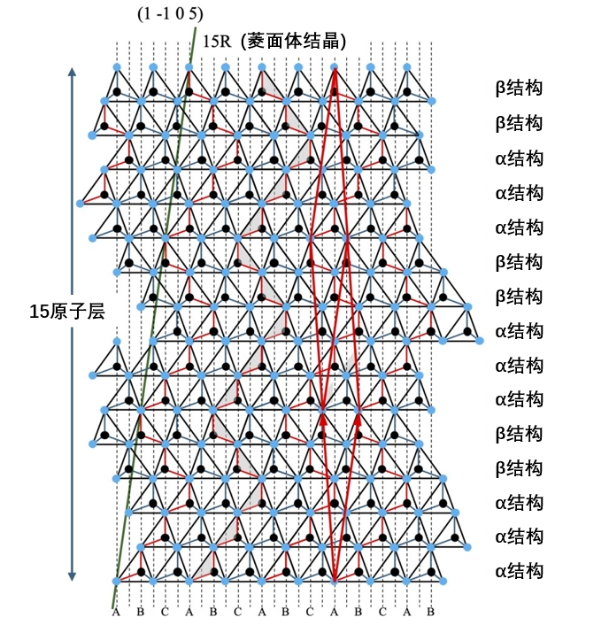 Figure 3-2. Stacked structure of 15R-SiC. Direction [0001] is shown above. The solid red lines (arrows) represent the reconstructed trigonal lattice and its basic translation vector.
Although it has been theorized that any stacking structure is possible, in fact, more than 200 crystal polymorphs have been found in SiC crystals, and all of them belong to the hexagonal or trigonal system (including 3C). However, even when attempts are made to simply prepare a particular polytype, it is difficult to succeed in most cases in terms of growth on the (0001) plane alone. As mentioned earlier, this is because the transformation of the layer structure between the α and β structures occurs in a sense by chance, and the maintenance of long periods or the accurate transfer of structural information far from the surface layer to the very top layer (such as structural information beyond 15 layers in 15R) is virtually impossible in probability. In particular, for periodicity beyond 8 layers, it can almost be said that it is extremely rare to occur naturally on a macroscopic scale. Polyforms such as 9R (Zhdanov notation (2-1) 3or (4-5)) are also theoretically possible, but have not been found to exist so far. In practice, the observed polytypes of 15R crystals are also mostly in the form of partial mixing in 4H or 6H crystals, which is just some kind of "defect" from the point of view of the polymorphism of the main crystal.
In the artificial preparation of 4H or 6H crystals, certain driving force conditions must be utilized that can effectively control the formation of β structures and realize crystals on a macroscopic scale. One of these methods is a “step-controlled epitaxy ” using atomic-level steps on a micro-inclined substrate. In conventional epitaxial growth, the formation of the upper layer will pass the structural information of the lower layer, so as to form the same crystal structure. However, when the diffusion length of the surface raw material species is sufficient, as shown in Figure 3-3, the raw material species will spread to the edge of the step and be absorbed by the crystal there, thus extending the step. This means that the epitaxial growth inherits not only the structural information of the base, but also the lateral structural information through the step edge, thus maintaining the layer structure as a whole.
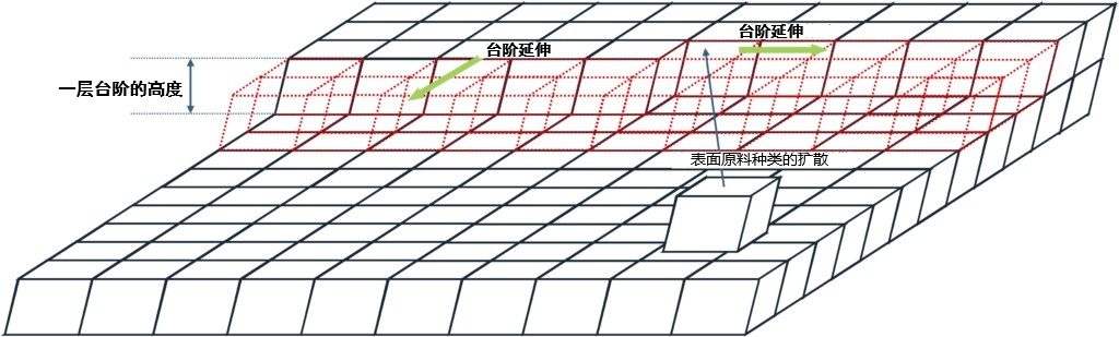
Figure 3-3. Step control epitaxy. Lateral structure information is also inherited through step edges.
In this kind of step control epitaxial growth, the declination angle (about a few degrees), the orientation and the lateral extension of the step, that is, the realization conditions of the layered growth are very important. In order to obtain a high-quality epitaxial film without other polytype mixing in the epitaxial growth of SiC, a declination angle of several degrees is usually required. Even in epitaxy growth of III-V group compound semiconductors, the (001) face substrate commonly used actually has a declination angle of about 0.1 degrees. However, when the stacking period becomes extremely long, the application on a macro scale obviously becomes difficult. Perhaps it is more reasonable to think of it as growth on an exponential plane other than the (0001) plane. Taking the 15R in Figure 3-2 as an example, there may be surfaces that are more likely to appear periodically, as shown by the solid green line. In this case, however, the layer structure will no longer have p 3m1 symmetry, but will become a rectangular net structure with significantly different aspect ratios and less symmetry, while the atomic-level flatness that is a prerequisite for layered growth will also deteriorate. This stacking will be more difficult to control than the (0001) plane.
Corundum Structure
Corundum structure is a structure commonly found in crystals of substances with an X2Y3 composition, such as alumina (Al2O3) and α-Ga2O3. Crystals of rubies and sapphires are typical examples of this structure. In the previous section, we used 15R-SiC as an example to explain the trigonal crystal system which forms rhombohedral lattice based on the hexagonal lattice stacking structure. So, what about the structure of corundum, which also belongs to the trigonal system?
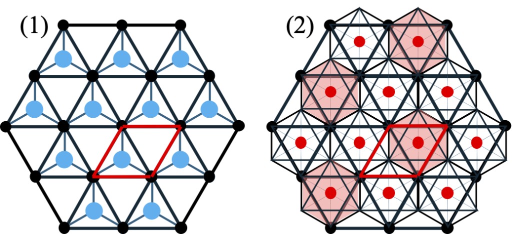
Figure 3-4. Hexagonal net and sites located in its vacancies. The light blue in (1) is the regular tetrahedron and the red in (2) is the octahedral sites. The red box is the basic cell of the hexagonal net. In (2), only 1/3 of the regular octahedral structure has been shaded for ease of observation.
Here is an analysis of the corundum structure. The HCP-based crystal structure mentioned earlier is made up of HCP and regular tetrahedral structure, while the corundum structure is HCP and regular octahedral structure. Figure 3-4 shows the two-dimensional hexagonal net and the relationship between regular tetrahedrons and regular octahedral present in the lattice point vacancies. In this figure, the barycentric positions of tetrahedral sites and octahedral sites are represented by light blue dots and red dots, respectively, while in the in-layer positions, the black dots correspond to the A site of the lattice, the light blue dots correspond to the B site, and the red dots correspond to the C site. The lattice points of the second layer (as A two-dimensional net) move to site B, and then accumulate in an alternating and repeating wurtzite arrangement of sites A and B. Note that, in the position perpendicular to the C-axis of the paper, the light blue dots are located at 1/4 of the distance between the layers, and the red dots are located at 1/2. In the regular octahedral structure, the position within the layer is equivalent to the C site in the regular tetrahedral structure, but the height is different. Figure 3-5 shows a cross section of the {11-20} face, with differences in atomic arrangement between the wurtzite type formed by the regular tetrahedral structure and the corundum type formed by the regular octahedral structure. Taking this into account, although the same HCP-based structure, in the corundum type, we also consider the vacancy layer (the green dot layer in Figure 3-5(2)) at the center of gravity position of the regular octahedral structure as a layer. In this way, the closest packing sites of HCP with coordinates (0, 0) and (2/3, 1/3) within the layers correspond to sites A and B in the hexagonal net, while the regular octahedral position points correspond to sites C. In crystal that places atom Y at sites A and B, and atom X at sites C, ACB 'C 'forms a periodic packing structure. This structure is known as the Nickel Arsenide structure, a close relative of corundum structure. In the wurtzite structure, no atoms are present at the C site, and in this structure, although the regular tetrahedral center of gravity at the vertex of the closest packing site has no atoms, the center of gravity of the opposite regular octahedron is occupied by atoms.
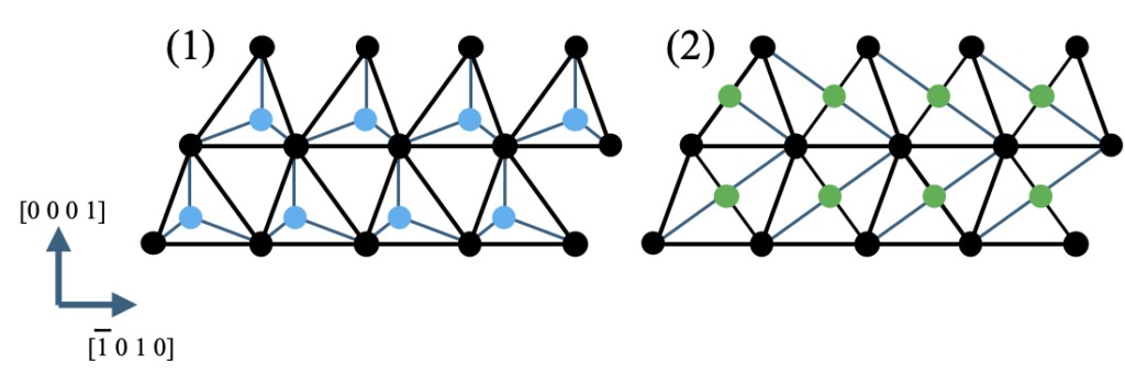
Figure 3-5. The barycentric position of the closest packing site of HCP as well as (1) regular tetrahedral structure and (2) regular octahedral structure. The figure is projected onto the {11-20} plane from the direction <11-20>. The wurtzite structure is formed when atoms are placed at the closest packing site represented by the black circle, and different atoms are placed at the position of the blue circle in (1); When different atoms are placed at the locations represented by the green circle in (2), the Nickel Arsenide structure is formed.
If this continues, the overall crystal structure will be a 4-layer period, but the situation becomes slightly more complicated because the composition of the matter in the corundum structure is not 1:1. If the structure of ACB 'C 'is followed, its crystal system will be similar to 4H-SiC, belonging to the hexagonal crystal system. However, since the X atom occupying the C site (in the case of Ga2O3, which is Ga) has a composition ratio of 2/3 that of the Y atom (in the case of Ga2O3, which is O), a vacancy of 1/3 will be created at the C site. In fact, if you extract the layer made up of X atoms at the C site, you will find that it exhibits the honeycomb structure shown in Figure 3-6. This result leads to the C site being divided into three types, known as the C,1 C2, and C3 sites. If the atomic species are ignored, the overall stacking structure becomes AC1B’C2’AC3B’C1’AC2B’C3’, i.e. one cycle consists of 12 layers.
It has already been shown how rhombohedral lattice form. This can be well understood by tracing the trajectory of C sites in the quasi-fundamental period ACB 'C' : every four layers of C sites change from C1→C2→C3→C1, which is very similar to the case of 15R, which forms rhombohedral lattice. In Ramsdell notation, this can be described as a 4-layer x 3-layer 12R structure.
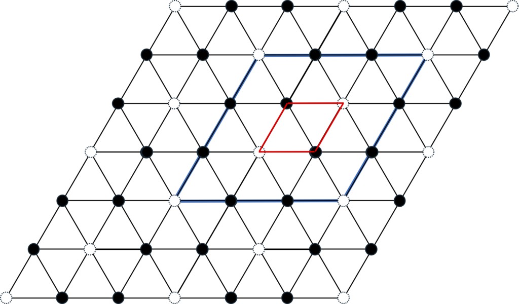
Figure 3-6. The atomic layer at site C in the corundum structure, as shown in the blue box, is only 1/3 (represented by the white circle) missing regularly and has a honeycomb-like structure, and the unit cell of this layer is three times the axial length.
The above describes how the corundum structure forms a rhombohedral lattice, and the result is an extremely long C-axis length with 12 layer periods. Although not around 15R, to artificially make a crystal with such a long period would require some kind of special driving force to maintain the said periodicity. In addition, one-third of the X atomic layer is missing, but to correctly form a regular honeycomb structure in a layer, as shown in Figure 3-6, it also requires considerable effort in crystallography.
Monoclinic Crystal Structure
So far, the cubic crystal system, hexagonal crystal system and trigonal crystal system have been introduced successively, and the monoclinic crystal system belonging to β-Ga2O3 will be introduced finally. Of the parallelepipedrons that make up a crystal, the lowest symmetry is the triclinic system, and the monoclinic system further restricts symmetry through lattice constant constraints (α = β = 90° or α = γ = 90°). Its symmetry is manifested by the existence of a double rotation axis orthogonal to the other two fundamental translation vectors, which is parallel to the third fundamental translation vector. In order to build a monoclinic crystal system model compatible with the packing structure from the two-dimensional network, two ways can be generally adopted as shown in Figure 3-7: (1) packing along the direction perpendicular to the grid plane on the basis of the orthorhombic lattice; And (2) based on a rectangular lattice, packing after translating along one of the basic translation vectors. Although the Bravais lattice eventually formed by both methods is a rhombic lattice, the difference should be noted. In Figure 3-7(1), the vertical stacking direction of the rhombic lattice surface is defined as the B-axis; In (2), one side of the non-oblong-shaped a-c faces (B-faces) is defined as the stacking direction (a-axis), both of which are β≠90˚.
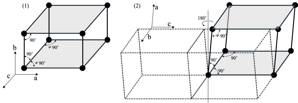
Figure 3-7. What a monoclinic lattice looks like from a two-dimensional lattice. (1) consists of a rhombic lattice with a b axis perpendicular to its net, and (2) consists of a rectangular lattice with an axis not perpendicular to its net. Because the a-c sides of the cell are not rectangular, β≠90˚. In (2), a dashed line is used to indicate that performing 2 rotations of the rectangular lattice face produces another A-axis and produces a field consisting of another cell that does not overlap the original cell.
When the stacking structure of the epitaxial layer is considered as the stacking structure of layers, it can be found that the most surface usually contains the symmetric element of double rotation axis. Under the transmission of this structural information, the upper layer will inherit the lower layer structure and form a monoclinic lattice. If this stacking conforms to the situation described in (2), two different crystal domains may be formed, which is reflected in Figure 3-7 (2). In the absence of other constraints, the two crystal domains are equally likely to form, and between them, the translational symmetry will be broken. In this case, to obtain epitaxial layered growth of a monoclinic system with fewer defect, a growth plane similar to that described in (1) should be chosen, where the growth plane is a rhombic lattice and the B-axis of the crystal is perpendicular to the growth plane (i.e., the net plane). This helps to stabilize the structure and reduce defect.
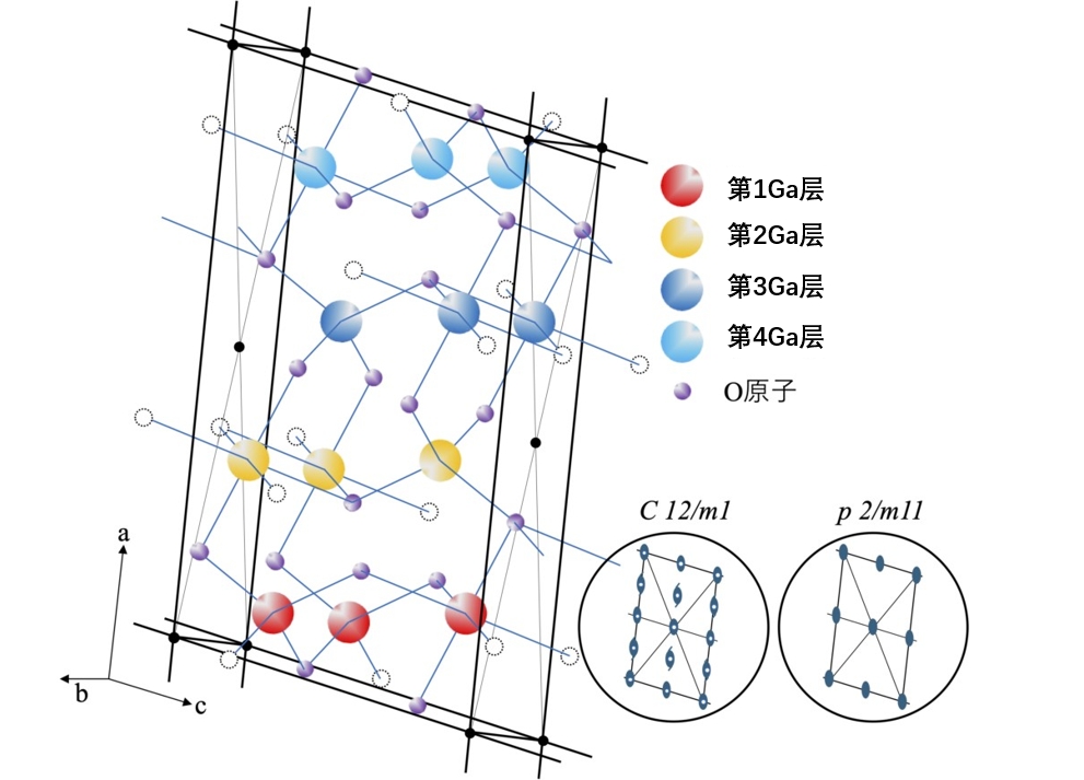
Figure 3-8. Crystal structure and cells of β-Ga2O3. This space group and the a-c planes are symmetric elements of the layer group when considered as layers (labeled only as the axis of rotation in the direction of the b axis). The axis is defined as β≠90˚. Black circles represent lattice points, and white circles (dashed lines) represent oxygen atoms in adjacent cells. There are 4 types of Ga atomic layers in the A-axis direction.
Let's take β-Ga2O3 as an example for analysis. The crystal structure of β-Ga2O3 is more complex than other structures, and it is a little difficult to understand and diagram, but we have modeled it in the way of Figure 3-8. For ease of understanding, the Ga atoms are drawn as larger dots and the O atoms as smaller dots. A striking feature of the structure is that both tetrahedral and octahedral structures are centered around the Ga atom and coexist in a 1:1 ratio within the unit cell (whereas in other semiconductors there is usually only one of these two structures). However, these structures are not regular polyhedra, with certain distortions, and are connected only by shared vertices or edges, with no shared faces. The unit lattice can be defined as a base-centered C lattice as shown in Figure 3-8 (i.e., A-B faces have a lattice point at their center), but in this case no atoms are present at the lattice point position.
In terms of lattice constants, β = 103.7°, and b:c:a ≈ 1:2:4, the difference between the three axis lengths is large. These axial length differences may be related to the number of atomic layers in the unit cell stacked along these axis directions. The basic element in the unit cell is Ga4O6, which corresponds to the structure of the base-centered lattice of C, and the unit cell contains two such basic units.
Next, we consider the stacked structure on the crystal face. First, consider the situation on the a-c planes, as shown in Figure 3-7 (1). The cell layers at growth time are almost the unit cells in Figure 3-8, and they can be stacked directly along the b axis. In this case, the tetrahedral structure with shared vertices and the octahedral structure with shared edges are connected in a zigzag pattern along the b axis and can be stacked without any offsets in the A-C planes. This situation is very similar to the <111> direction of the FCC structure. However, because the unit cell is very large and contains a large number of atoms, it can become more difficult to accurately reproduce the complex structure within the layer (containing only the double rotating axisymmetric elements).
On the other hand, what about the growth of the b-c planes? This situation is similar to Figure 3-7 (2), where the A-axis is not perpendicular to the b-c plane. Therefore, it is easy to generate different crystal domains as described in Figure 2-7 (2). In this stacked structure, the unit cell consists of 4 layers, but layers 2 and 4 are the structure of layers 1 and 3 after they are rotated 180° about the B-axis. Due to the binding direction, the stacking requires displacement within the layers, and due to the instability of the binding direction of the oxygen atoms, the polyhedral structure is distorted, which makes the displacement amount in the direction of the C-axis not constant between the layers. Considering the layer structure changes in the HCP base structure, this change may lead to the generation of defect. Therefore, we expect stacks on the c plane to have a high probability of defect occurring.
To sum up, compared with other semiconductor crystals, β-Ga2O3 requires some special driving mechanism to stabilize its structure in the growth of crystals with high quality and few defect. It is particularly important to find and control this mechanism. It is already known that at the most surface layer of the (-201) face, whose structure is somewhat similar to the wurtzite type (0001) face, there may be a way to efficiently exploit this property.
Summary
In this series, although no rigorous academic analysis is carried out, the characteristics of semiconductor crystals are reviewed from the perspective of advances in semiconductor technology, and in particular revisited from the perspective of symmetry and stacking structure. As shown in Figure 3-9, the general development trend of semiconductor technology can be seen: from elemental semiconductor → 1:1 composite semiconductor → 2:3 composite semiconductor, to cubic crystal system → hexagonal crystal system → trigonal crystal system. Reviewing the changes in semiconductor crystal structure, it can be clearly seen that although the driving force of technological progress is great, it is undeniable that semiconductor materials are developing towards more complex crystal structures. Just as the "crystal symmetry" discussed in the paper, this is one aspect of its "complexity", and the quality of the symmetry in engineering has a direct impact on the quality of the crystal (such as the existence of the crystal defect).
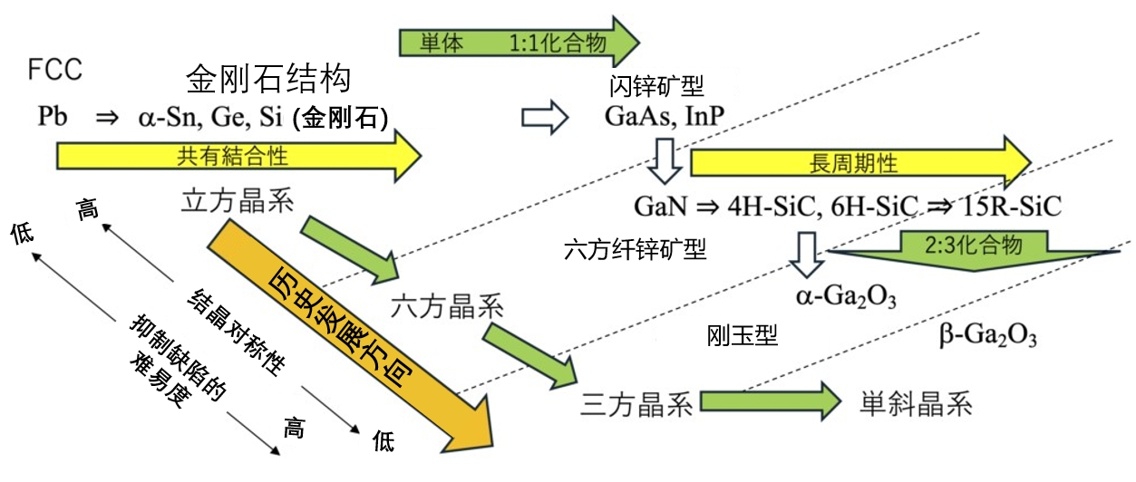
Figure 3-9 Crystal structure relationships among various semiconducting materials.
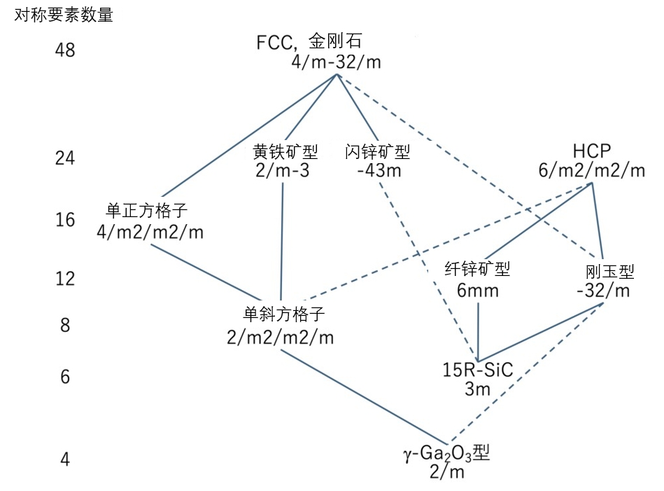
Figure 3-10 Inclusion relationship of crystal point groups of various semiconductor crystal structures. The solid line shows the normal subgroups, and the dashed line shows the conjugated subgroup relationships. Crystal point groups are represented by international symbols.
The symmetry of a crystal is mathematically characterized by the space group, or point group, to which the crystal structure belongs. The crystal structures involved in this paper include FCC, HCP, Diamond structure, Zincblende type structure, Wurtzite type structure and Corundum structure, etc. Finally, we show the point group symmetry hierarchy of these structures through Figure 3-10, and list the number of symmetry operations. Mathematically speaking, this is the relationship between "partial group" and "supergroup". A similar relationship is partially true (and partially not true) for space groups, but it is too complicated for the author to understand, so this article will not delve into it. In any case, as the level goes down, symmetry operations gradually decrease, which means that, as mentioned at the beginning of the article, unit cells in the crystal are increasingly difficult to maintain in the same pattern.
As a semiconductor technology, the performance of the chip in a semiconductor device is the embodiment of its value. Although the performance of semiconductor device chips is proven, the demand and development drive for higher quality crystal technology are often overlooked in the pursuit of performance. Nowadays, as the requirements of semiconductor technology continue to increase, the specifications of device chips are becoming more and more complex. History suggests that new semiconductor technologies will require more complex crystal structures. Making more complex crystal structures is bound to be accompanied by more difficulties. The "crystallinity" of crystals lies in translational symmetry. Some practical cases are presented to show that in order to maintain translational symmetry without defect during crystal growth, corresponding driving forces must be provided. The mechanism of this driving force needs to be discovered and controlled, which can only be developed through knowledge and experience of crystal engineering, requiring more refined and superior techniques. These techniques will help to greatly improve the quality of semiconductor crystals and enable higher quality semiconductor materials in the future. Crystal engineering will play an increasingly important role in semiconductor technology. It is the talents in this field who will take on this important task.
