


Member News
【Member News】Suzhou Nanotechnology Institute's Processing Platform and Nanodevice Research Department Make New Progress in the Field of Solar-Blind UV Detection
日期:2025-03-25阅读:1021
Solar-blind UV detection technology has become a key technology in astrophysical observation, high-voltage power monitoring, forest fire prevention, national high-tech application and other fields because of its high signal-to-noise ratio and low false alarm rate. Traditional silicon-based detectors are limited by material characteristics and need to realize Solar-blind band recognition through complex optical filter system, which leads to heavy equipment, high cost and insufficient radiation resistance. Gallium Oxide (Ga2O3), an ultra-wide band gap semiconductor with a bandgap of ~ 4.9eV, is a natural solar-blind detection material in the ultraviolet band (200-280 nm). Its 254 nm spectral cutoff feature enables ultra-high signal-to-noise ratio detection without the need for external optical filters. In addition, Ga2O3 single crystal can be prepared by mature technology such as melt method in recent years, so that it has both low cost mass production potential and excellent anti-irradiation performance, which provides a solid foundation for the construction of lightweight, high performance, large array solar-blind UV detector integrated chips.
Based on the collaborative innovation of Gallium Oxide detector array optimization and intelligent circuit design, the Nanocrystalline Processing Platform of Suzhou Institute of Nano-Tech and Nano-Bionics, CAS and the relevant team of the Research Department of Nanodevices have made an important breakthrough in the field of solar-blind ultraviolet detection.
Ultrasensitive Dynamic Ultraviolet Imaging Based on a Ga2O3 Photodetector Array
In this work, by reducing the triethylgallium flow from 200 sccm to 50 sccm, oxygen vacancy was effectively suppressed, leading to a transition in noise from Lorentzian to flicker-type, with a significant decrease in noise current from 0.15 nA to 1.01 pA. This improvement enhanced the detector’s performance, yielding high sensitivity (3.72 A/W), fast response time (τd1/τd2 = 1.6/13 ms), and solar-blind detection characteristics. In terms of circuit design, the team of Song Helun in the Device Department built a "four-in-one" signal processing system -- using a low on-resistance switch array to achieve pixel precision gating, a transconductance amplifier circuit to complete nA level weak signal amplification, a high-significant digit ADC low-noise signal acquisition, combined with high-speed parallel processing of FPGA chips, to form a complete imaging circuit solution. Based on this development, the 8×8 pixel array imaging system can identify the weak ultraviolet signal of 2.6 μW/cm2 3 meters away in the natural light environment, and capture the trajectory of the moving point light source in real time (such as the simulation of the tail flame of the aircraft). It provides a new paradigm of miniaturized and highly reliable solar-blind UV imaging technology for the national high-tech field and civil fire monitoring.
The results were published in the internationally renowned journal Optics Letters under the title of Ultrasensitive dynamic ultraviolet imaging based on Ga2O3 photodetector array (50, 2025 (5), pp. 1633-1636, https://doi.org/10.1364/OL.555862). The first author is Chen Tiwei, a doctoral student at the University of Science and Technology of China, and the corresponding authors are Zhang Baoshun and Song Helun.
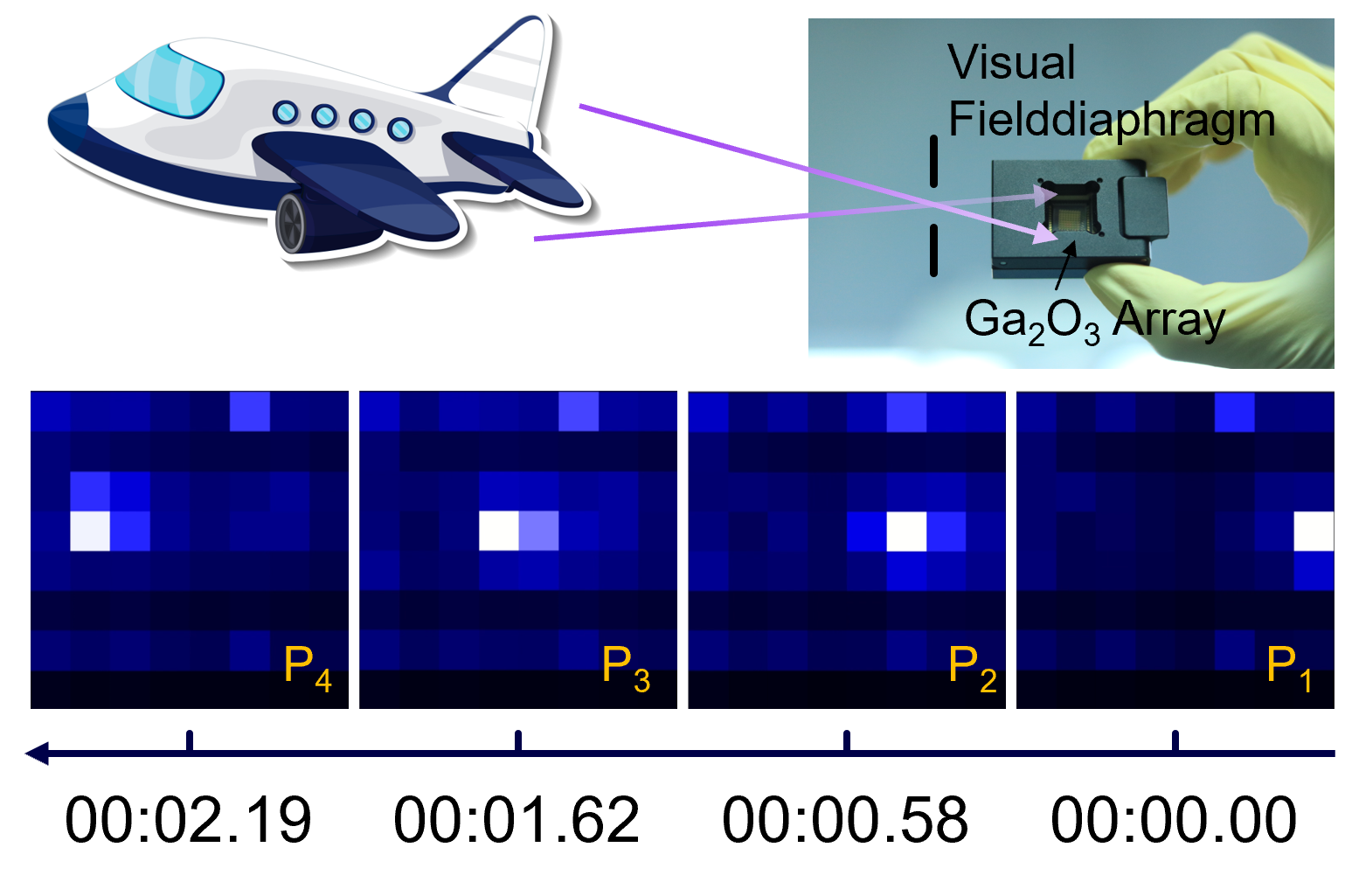
FIG. 1. Schematic diagram of UV dynamic imaging test scheme and display window of upper computer software
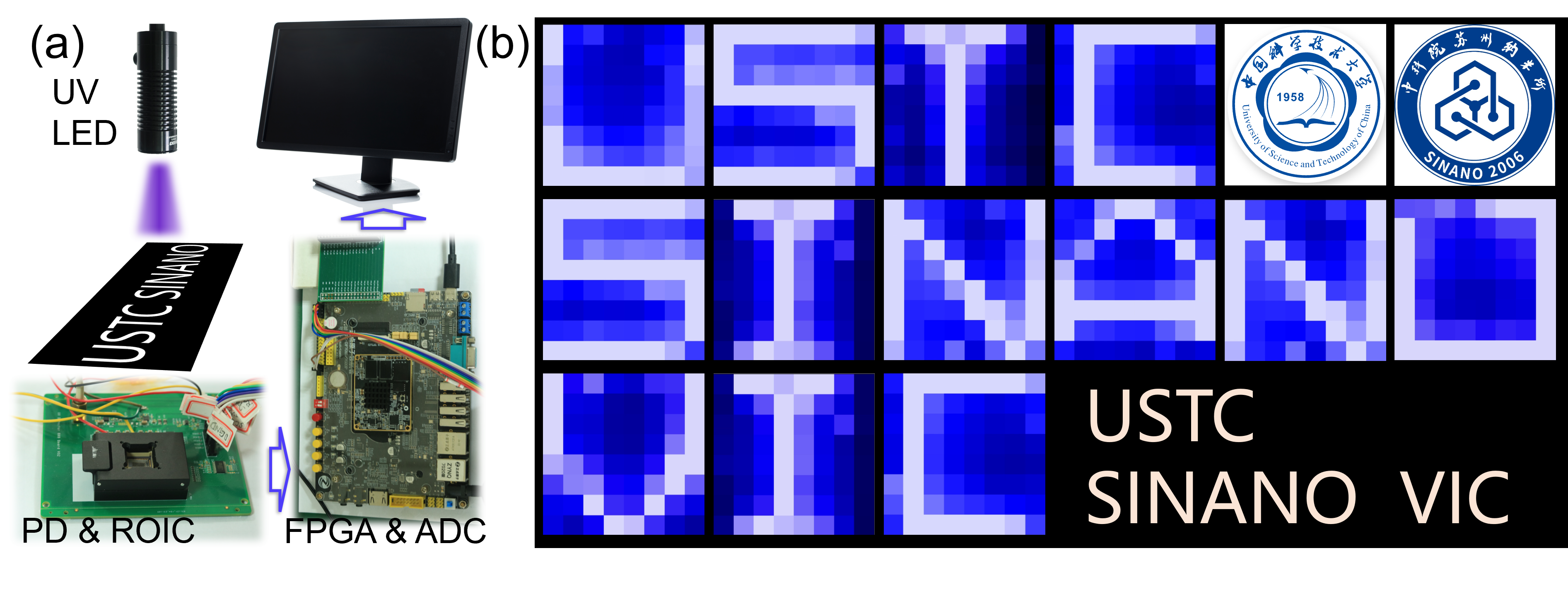
Figure 2. Schematic diagram of the prototype of the UV imaging system and the display effect of the UV imaging system
In recent years, the nanomachning platform has focused on the national strategic demand of ultra-wide band gap semiconductor materials and devices to capture the new round of material technology which is about chips, provided technical support for the development of Gallium Oxide (Ga2O3) thin film epitaxy and device technology of ultra-wide band gap semiconductors, overcome the sensitivity, speed and integration of Gallium Oxide ultraviolet detector and other problems, and recently made a series of new breakthroughs:
Low-Power Detector Breakthrough: GaON Dielectric Layer to Achieve a 20-Fold Jump in Responsivity
Aiming at the bottleneck of low sensitivity of self-driven detector, the research team grew multi-crystalline phase Ga2O3 thin films on p-GaN substrate by MOCVD technology, and innovatively introduced in-situ GaON dielectric layer, which significantly improved the photogenerated carrier separation efficiency. The device achieves 3.8A /W ultra-high responsivity (254 nm illumination) at 0 V bias, dark current as low as 3.08 pA, detectivity of 1.12×10¹⁴ Jones, response speed of 66/36 ms, and response speed without external power supply. The achievement provides a miniaturized solution for passive scenarios such as deep space exploration and field monitoring.
The results is published under the title of High-Photoresponsivity Self-Powered a‑,ε‑,and β‑Ga2O3/p-GaN Heterojunction UV Photodetectors with an In Situ GaON Layer by MOCVD in the journal ACS Applied Materials & Interfaces (2022, 14 (30), 35194-35204. https://doi.org/10.1021/acsami.2c06927). The first author is Ma Yongjian, a doctoral student at the University of Science and Technology of China, and corresponding authors are Zhang Xiaodong and Fu Houqiang.
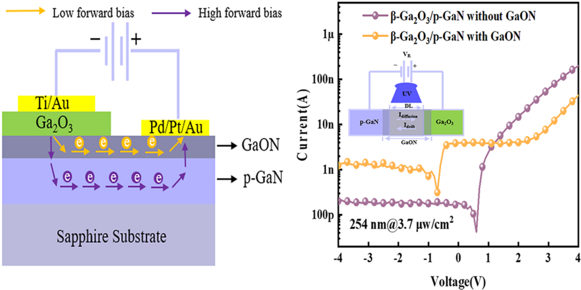
FIG. 3. Schematic diagram of in-situ GaON dielectric layer enhanced photocurrent and device 254-nm illumination I-V characteristic curve
High-Speed High-Frequency Detector: the Nano Seed Layer Inhibits Defect, and the Bandwidth Breaks Through 2 kHz
In order to improve the device response speed, the team proposed and designed the single crystal Ga2O3 nanoparticle seed layer (NPSL) during the epitaxial growth of MOCVD on 4-inch Sapphire substrate, optimizing the film growth mode from island growth to horizontal merging, effectively inhibiting deep level defect such as oxygen gap. The prepared metal-semiconductor-metal (MSM) structure detector has a dark current of only 81.03 pA, a response speed of 62/142 μs, a frequency bandwidth of 2 kHz, a detection rate of 2.81×10¹⁴ Jones, and a linear dynamic range of 61 dB, which can meet the needs of high-speed communication and transient signal capture.
The relevant paper is published under the title of High-Speed and Ultrasensitive Solar-Blind Ultraviolet Photodetectors Based on In Situ Grown β‑Ga2O3 Single-Crystal Films in the journal ACS Applied Materials & Interfaces (2024 (5), 6068-6077. https://doi.org/10.1021/acsami.3c15561), The first author is Chen Tiwei, a PhD student at the University of Science and Technology of China, and corresponding authors are Zhang Baoshun and Li Shaojuan.
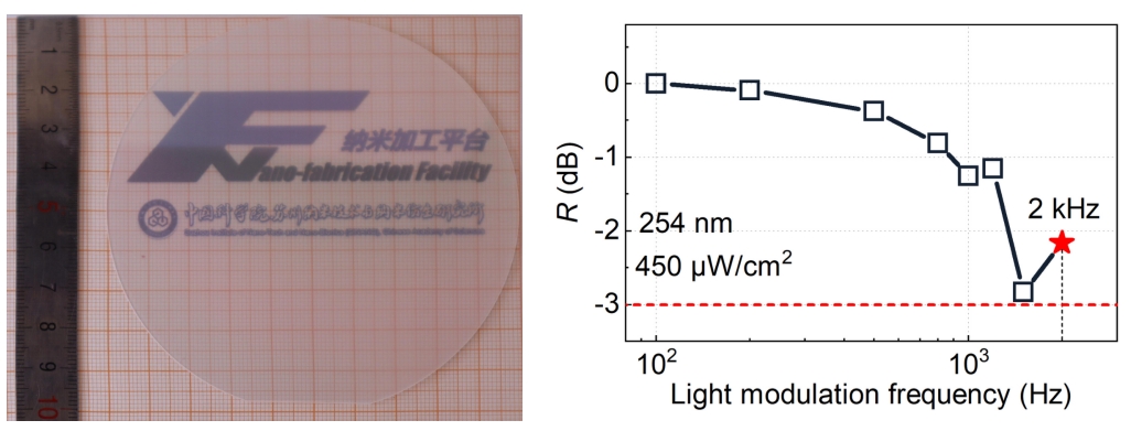
Figure 4. (a) Ga2O3 epitaxial wafer on a 4 inch Sapphrie substrate, (b) Ga2O3 MSM detector frequency response bandwidth
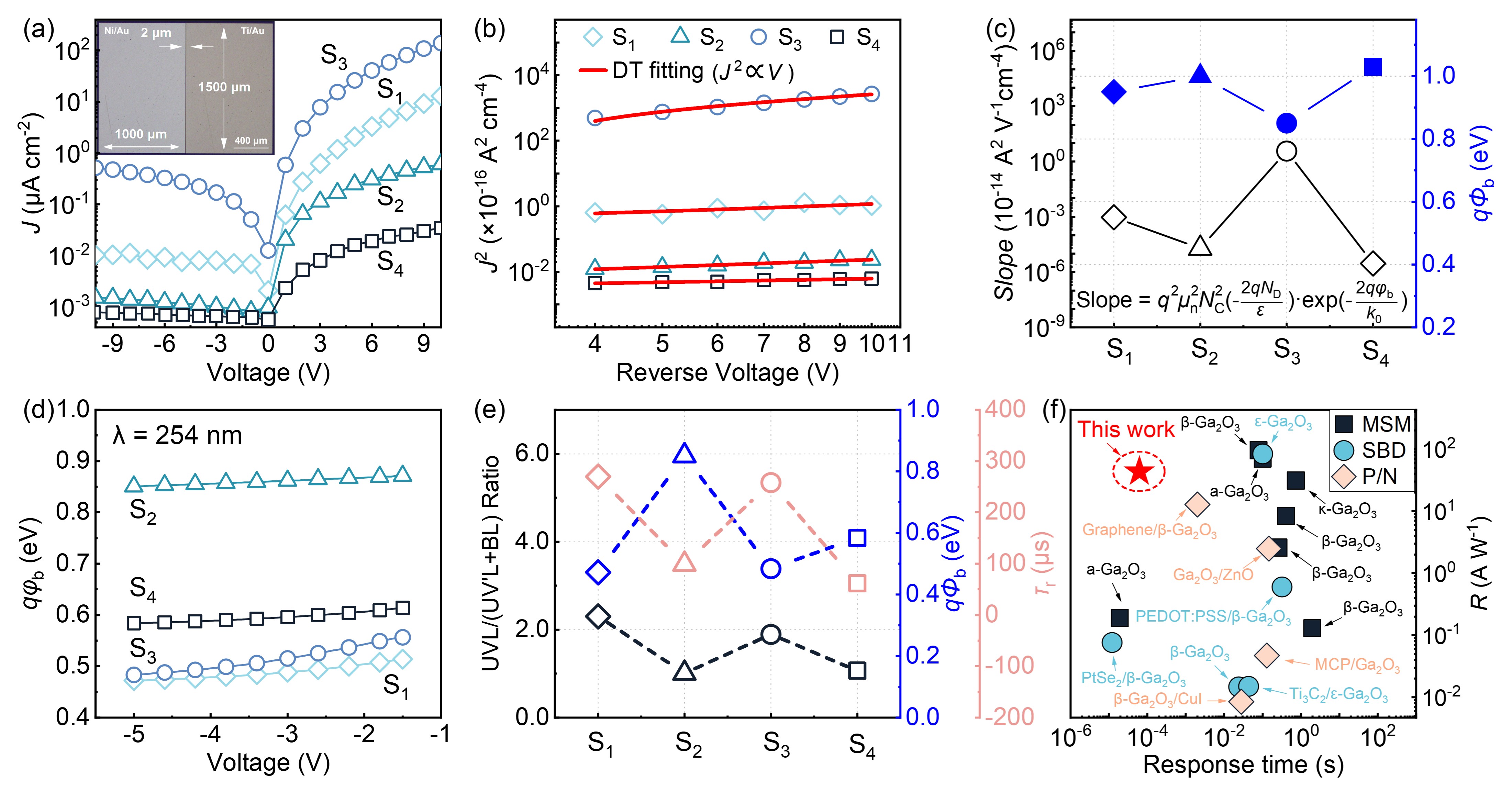
Figure 5. Schottky barrier and defect gain analysis based on diffusion theory
Ga2O3 Schottky Detector with Quasi-Vertical Structure: High Speed and High Responsiveness
To meet the national high precision detection needs, the research team by shortening the carrier migration path and optimizing the electrode design, based on the Pt low electrode epitaxy growth of the quasi-vertical structure Ga2O3 Schottky UV detector, the introduction of the photosensitive zone embedded metal fringe design, the responsiveness increased to 2998 A/W, response time up to 120 μs. It provides a new solution for high-precision detection applications such as airborne detection and ozone monitoring.
The relevant result was published in the journal IEEE Electron Device Letters under the title of High-Speed and High-Responsivity Quasi-Vertical Schottky Photodetectors of Epitaxial Ga2O3 on Pt Substrate (2025 46-48 (1), 60-63, https://doi.org/10.1109/LED.2024.3496557).The first author is Zhang Huanyu, a master's student at the University of Science and Technology of China, and the corresponding authors are Zhang Xiaodong and Zeng Chunhong.
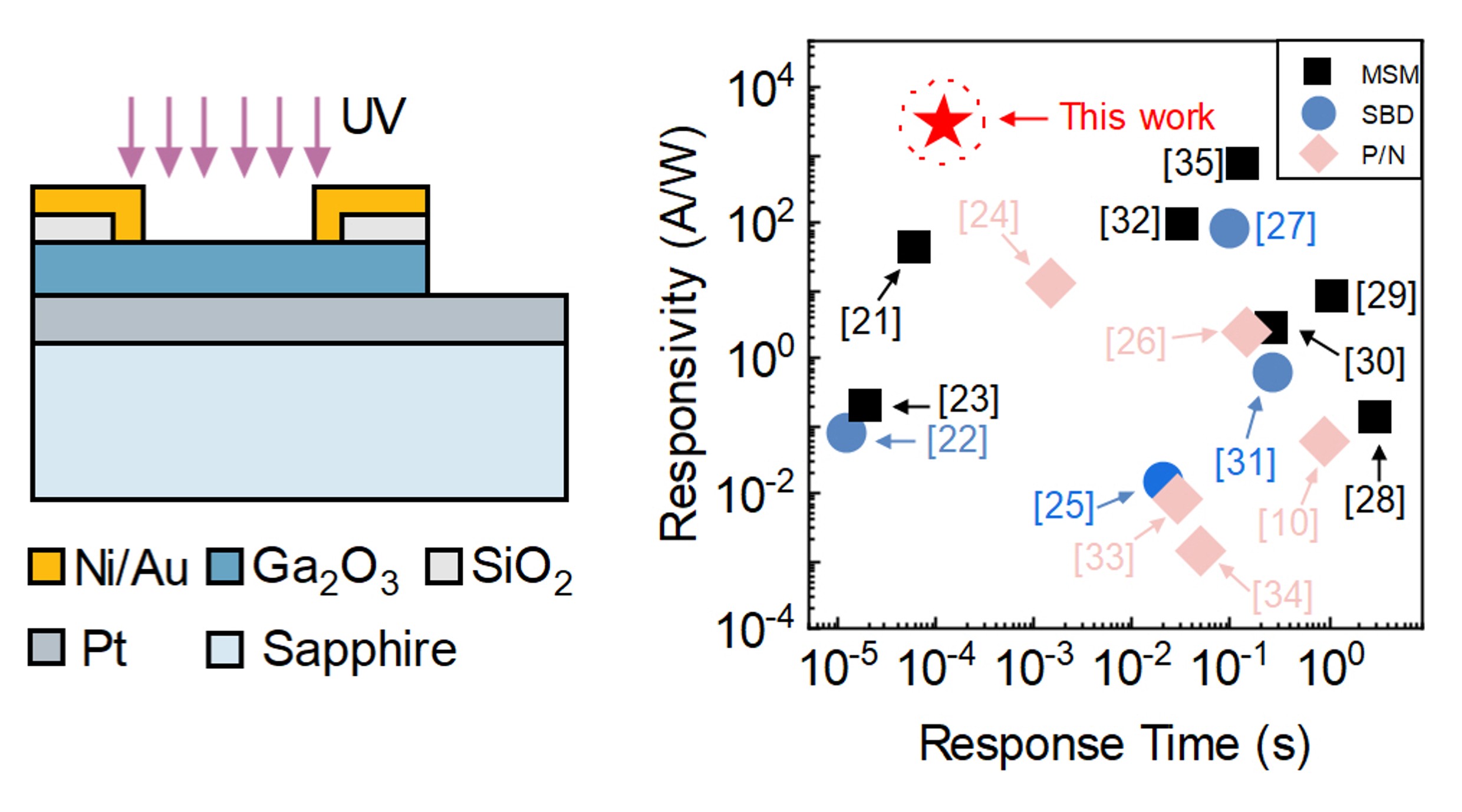
FIG. 6. Comparison of quasi-vertical Pt/Ga2O3 Schottky photodetector and its core parameters
The above series of achievements have promoted the development of Gallium Oxide solar-blind ultraviolet detector to the direction of high sensitivity, low power consumption and miniaturization, which has great application value and technical advantages in environmental monitoring, biomedicine, deep space exploration, national high-tech applications and other fields. The above work has been supported by the National Key Research and Development Program, the National Natural Science Foundation of China, the Natural Science Foundation of Jiangxi Province, the construction project of Nanchang Key Laboratory, etc. At the same time, it has been strongly supported by the Nano-processing platform, test and analysis platform, Nano-Device Research Department, Nano-Vacuum Interconnect Experimental Station (Nano-X) and other departments of Suzhou Institute of Nano Engineering, Chinese Academy of Sciences.
