


News Trends
【World Express】The Research Team at the University of Tokyo Developed Gallium Oxide for UWBG Semiconductors, Opening Up Possibilities for Optical Devices
日期:2024-11-27阅读:1147
Recently, a research team from Research Center for Advanced Science and Technology, The University of Tokyo, successfully realized the use of metastable phase α-Ga2O3 of Gallium Oxide to fabricate single-mode waveguides and observe optical guided waves. The team proposes to use α-Ga2O3, which has not been fully studied, as a new optical circuit platform for photonics materials. The α-Ga2O3 was grown on sapphire substrate by Mist Chemical Vapor Deposition (Mist CVD) method, and the waveguide structure was fabricated by reactive ion etching. The optical guided wave was observed by grating coupler. At present, the research team has successfully realized the fabrication of single mode waveguides for red light (wavelength 633nm) and green light (wavelength 532nm) and the observation of optical guided waves.
Gallium Oxide for Optical Devices
Because of the characteristics of high withstand voltage and low loss, Gallium Oxide has a broad application prospect in the field of power converters and switching devices requiring high voltage. In addition, due to the transparency of Gallium Oxide in the deep ultraviolet to near infrared region, its use as a platform for optical circuits at different wavelengths has also been investigated.
Researchers from the Research Center for Advanced Science and Technology, The University of Tokyo mentioned: "At present, amorphous Silicon Nitride (SiN) is widely used as a material for visible optical waveguides, but its composition and strain need to be controlled. In this study, we believe that the use of crystalline Gallium Oxide as optical waveguide material can more easily obtain stable optical properties. In addition, Gallium Oxide also has a function as a semiconductor material, so it is expected to fuse with various active elements in the future."
Gallium Oxide has several different orientation (※1), of which the most stable phase is β-Ga2O3 which was first studied as a visible optical waveguide. However, the study of β-Ga2O3 wave guides has not made enough progress, and the single-mode characteristics (※2) have not been fully discussed, and the realization of high-efficiency optical waveguides remains a challenge. On the other hand, research on optical circuits using metastable phase has stalled, so need to development from a broader perspective. One of them, the metastable phase α-Ga2O3, has a wider bandgap (5.3eV) and a higher refractive index than β-Ga2O3 and may exhibit superior performance on optical circuit platforms.
※1 Orientation: the specific structure of a substance when it exists as a crystal. Depends on the type and symmetry of the regular arrangement of atoms and molecules (lattice).
※2 Single Mode: A state in which light travels in a specific mode in optical transmission devices such as fibers and waveguides.
Mist-CVD Technology Can Achieve Large Area and High-Quality Growth of Gallium Oxide Films.
Based on this background, the researchers focused on the metastable phase α-Ga2O3, mainly trying to make single-mode waveguides in the visible region and observe the optical guided waves. This research aims to exploit the excellent optical properties of Gallium Oxide to explore its potential as a platform for next-generation optical circuit devices.
In the experiment, a high-quality α-Ga2O3 film with a thickness of about 200nm was first grown on a C-face sapphire substrate using the Mist-CVD method. The Mist-CVD method is a method of growing the film by chemical reaction by supplying a Mist precursor solution to a preheated substrate. The process does not require a vacuum environment, so it has the advantage of reducing costs during manufacturing. The researchers explained: "By using the Mist-CVD method, high quality α-Ga2O3 films can be prepared at relatively low temperatures. In addition, it is possible to form very high-quality films on sapphire substrates."
Next, the team used Plasma Enhanced Chemical Vapor Deposition (PECVD) (※3) to form a Silicon Dioxide (SiO2) sacrifice layer on the α-Ga2O3 film. The Nickel (Ni) mask was then made using the photoetching technology. By using the mask, mixed gas Reactive Ion Etching (RIE), using Boron Chloride (BCl3) and Chlorine (Cl2) mixed gas, the single mode waveguide structure was successfully formed. Finally, the SiO2 sacrificial layer and Ni mask were removed by Hydrofluoric Acid (HF) to complete the fabrication of the waveguide structure. The resulting waveguide has a high mesa structure with a width of 1μm and is equipped with grating couplers at both ends (shown in Figure 1). The researchers added: "In order to integrate the grating couplers that need to be manufactured at sub-wavelength scales into the waveguide, we used Nickel, which has excellent etching resistance, as a mask to fabricate the device. In addition, the coupling technique of spatial mode to waveguide mode achieved by grating couplers has a higher tolerance for position deviation than the end face coupling, and has good compatibility with the automatic testing of waveguides, so this technique is important for industrial applications."
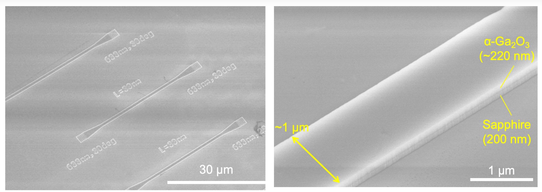
Figure 1. SEM image of the fabricated waveguide. (left) top view and (right) enlarged view.
※3 PECVD Method: A type of Chemical Vapor Deposition (CVD) method. A technique that uses plasma to accelerate a chemical reaction and deposit a film on a substrate.
After calculating the intrinsic mode based on the waveguide structure parameters measured by scanning electron microscope (SEM) (※4), the structure is confirmed as a single mode waveguide of TE polarization by the derived dispersion curve. Subsequently, a red laser with a wavelength of 633 nm was vertically incident on one side of the grating coupler at the end of the waveguide using a space optics system, and light emitted from the grating coupler on the other side was observed (Figure 2).
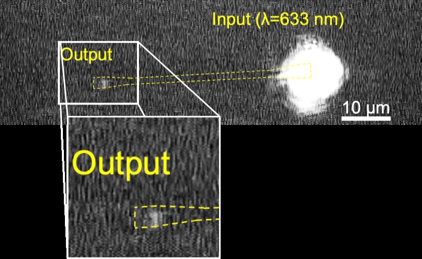
Figure 2. shows a CCD image of the optical waveguide.
※4 SEM Measurement: Scanning electron microscopy (SEM) is used to measure the size and shape of the microstructure.
Verification of Gallium Oxide Curved Waveguides
A curved waveguide with a bending radius of 20 µm has been successfully fabricated by a similar process. For this structure, after feeding red light of Y-polarized light to a grating coupler, it was observed that the grating coupler emitted X-polarized light on the other side (Figure 3). This result confirms the characteristic of TE polarized optical waveguide calculated by intrinsic mode.
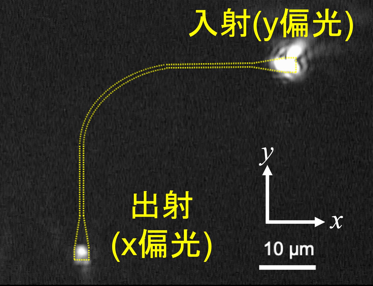
Figure 3 shows a CCD image of the waveguide in a curved waveguide.
"By reducing the surface roughness (surface unevenness and micro-concave-convex structure), light loss and scattering can be further suppressed," the researchers note. In future studies, it is planned to improve the waveguide performance by reducing the side wall roughness and improving the technology, with the goal of developing a lower loss and more efficient optical waveguide.
It is expected that this ultra-wide bandgap semiconductor property of Gallium Oxide materials will be exploited in the future to develop innovative optical devices. This study demonstrates the potential of Gallium Oxide as an excellent waveguide material. Due to its ability to manufacture small waveguides, it can be expected to have a wide range of applications using near ultraviolet to visible light, including on-chip biosensors (※5). If higher quality crystals can be obtained, Gallium Oxide has the potential to demonstrate properties beyond those of conventional materials.
※5 On-Chip Biosensor: A tiny biosensor integrated on a semiconductor chip. Biosensor is a sensing device that detects chemicals and biomolecules and converts them into measurable outputs (such as electrical and light signals).
